NVIDIA Discloses Next-Generation Tegra SoC; Parker Inbound?
by Joshua Ho on January 5, 2016 4:31 AM EST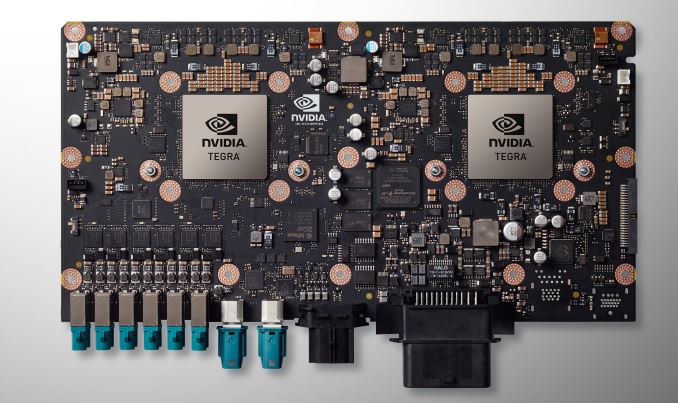
While NVIDIA has been rather quiet about the SoC portion of the DRIVE PX 2, it’s unmistakable that a new iteration of the Tegra SoC is present.
The GPUs and SoCs of the DRIVE PX 2 are fabricated on TSMC’s 16nm FinFET processes, which is something that we haven’t seen yet from NVIDIA. The other obvious difference is the CPU configuration. While Tegra X1 had four Cortex A57s and four Cortex A53s, this new SoC (Tegra P1?) has four Cortex A57s and two Denver CPUs. As of now it isn’t clear whether this is the same iteration of the Denver architecture that we saw in the Tegra K1. However, regardless of what architecture it is we’re still looking at a CPU architecture that is at least partially an ARM in-order core with a wide, out of order VLIW core that relies on dynamic code optimization to translate ARM instructions into the VLIW core ISA.
Based on the description of the SoC, while NVIDIA is not formally announcing this new SoC or giving it a name at this time, the feature set lines up fairly well with the original plans for the SoC known as Parker. Before it was bumped to make room for Tegra X1, it had been revealed that Parker would be NVIDIA's first 16nm FinFET SoC, and would contain Denver CPU cores, just like this new SoC.
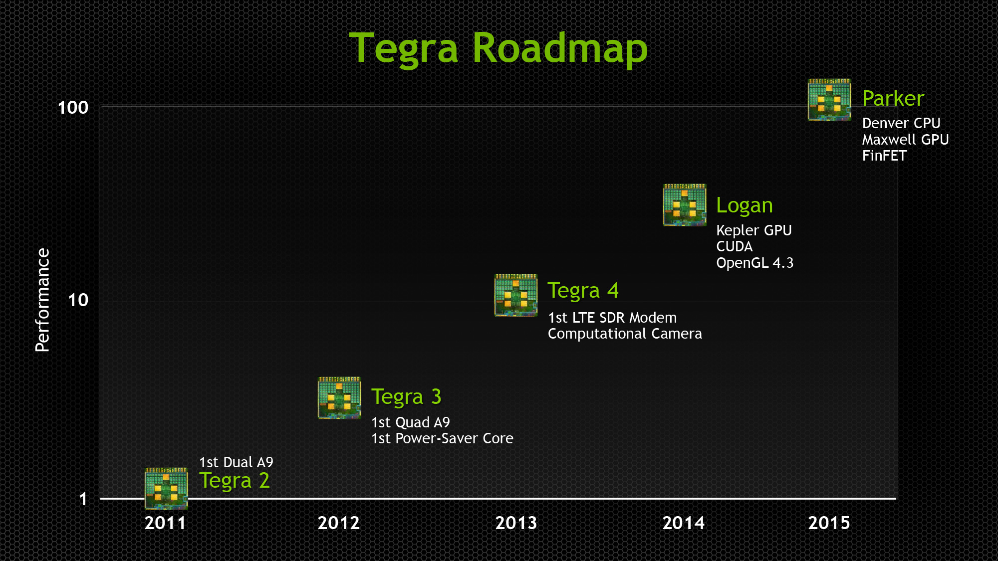
NVIDIA's Original 2013 Tegra Roadmap, The Last Sighting of Parker
Of course Parker was also said to include a Maxwell GPU, whereas NVIDIA has confirmed that this new Tegra is Pascal based. Though with Parker's apparent delay, an upgrade to Pascal makes some sense here. Otherwise we have limited information on the GPU at present besides its Pascal heritage; NVIDIA is not disclosing anything about the number of CUDA cores or other features.
| NVIDIA Tegra Specification Comparison | ||||
| X1 | 2016 "Parker" | |||
| CPU Cores | 4x ARM Cortex A57 + 4x ARM Cortex A53 |
2x NVIDIA Denver + 4x ARM Cortex A57 |
||
| CUDA Cores | 256 | ? | ||
| Memory Clock | 1600MHz (LPDDR4) | ? | ||
| Memory Bus Width | 64-bit | ? | ||
| FP16 Peak | 1024 GFLOPS | ? | ||
| FP32 Peak | 512 GFLOPS | ? | ||
| GPU Architecture | Maxwell | Pascal | ||
| Manufacturing Process | TSMC 20nm SoC | TSMC 16nm FinFET | ||
But for now the bigger story is the new Tegra's CPU configuration. Needless to say, this is at least somewhat of an oddball architecture. As Denver is a custom CPU core, we’re looking at a custom interconnect by NVIDIA to make the Cortex A57 and Denver cores work together. The question then is why would NVIDIA want to pair up Denver CPU cores with also relatively high performng Cortex A57 cores?
At least part of the answer is going to rely on whether NVIDIA’s software stack either uses the two clusters in a cluster migration scheme or some kind of HMP scheme. Comments made by NVIDIA during their press conference indicate that they believe the Denver cores on the new Tegra will offer better single-threaded performance than the A57s. Without knowing more about the version of Denver in the new Tegra, this is somewhat surprising as it’s pretty much public that Denver has had issues when dealing with code that doesn’t resemble a non-branching loop, and more troublesome yet code generation for Denver can take up a pretty significant amount of time. As we saw with the Denver TK1, Cortex A57s can actually be faster clock for clock if the code is particularly unfavorable to Denver.
Consequently, if NVIDIA is using a traditional cluster migration or HMP scheme where Denver is treated as a consistently faster core in all scenarios, I would be at least slightly concerned if NVIDIA decided to ship this configuration with the same iteration of Denver as in the Tegra K1. Though equally likely, NVIDIA has had over a year to refine Denver and may be rolling out an updated (and presumably faster) version for the new Tegra. Otherwise it also wouldn’t surprise me if the vast majority of CPU work for PX 2 is run on the A57 cluster while the Denver cluster is treated as a co-processor of sorts, in which only specific cases can even access the Denver CPUs.


23 Comments
View All Comments
hans_ober - Tuesday, January 5, 2016 - link
It's possible that they'll use the Denver part for repetitive optimized tasks and A57 for the other. I doubt this is even gonna be in a phone/tablet, they've got rid of the power saving cores. Looks like this has been designed ground up for automotive applications.Mobile-Dom - Tuesday, January 5, 2016 - link
Why on earth would they use the A57's at this point? when A72 i out and, well better, and they have their own core, if youre going custom, go fully custom, if not, use the newest and high performing Core.PaulJeff - Tuesday, January 5, 2016 - link
The A57 is used *with* the Denver cores, so they are probably used as companion cores for specific threads or operations. On top of that, Nvidia is most likely building a custom version of Android or custom kernel to run this hardware. With full control over the hardware and software layers, they can leverage the strengths of the A57.Also, we can speculate that the A72 was either too new for Nvidia when they started this project or the A57 is better suited for their use case.
Remember, this is for automotive use, not mobile devices.
jasonelmore - Tuesday, January 5, 2016 - link
yeah i'm not a fan of denver's code morphing architecture.. I wish they would ditch the concept all togather.jjj - Tuesday, January 5, 2016 - link
I hoped they would do this and run the new code on the ARM core (hoped A72 but , oh well) while also translating it for Denver so the next time it can run on Denver. Remains to be seen how they do power management,might have been easier to just give Denver a short clock boost when dealing with new code.Then again ,they don't get any wins so it matters less.
yannigr2 - Tuesday, January 5, 2016 - link
The SOCs used in this board could just meant for that board and not used anywhere else, like tablets. So knowing that those SOCs will be used in self driving cars, and considering the possibility Nvidia to also offer the software for that usage, then probably for that specific software and those specific tasks, Denver cores are better than A57s.jjj - Tuesday, January 5, 2016 - link
If it was just for cars they would have detailed it today but they seem to have delayed the reveal for MWC. They can't really afford to make a chip just for auto for now anyway, they need to try and get some extra revenue from elsewhere.yannigr2 - Tuesday, January 5, 2016 - link
No they don't have to detail it today or even tomorrow. Those who are going to care about this are those in big offices in car companies. Those are the people who will be informed about it. Not the end user. The end user will just learn from commercials that this car is a magical car and nothing more. That customer is a car driver not a computer user.Hans de Vries - Tuesday, January 5, 2016 - link
Tegra PX targeted at both the Console and Automotive sector would make sense. It would need sufficient performance to allow porting of current Console games and, very important, get Game designers interested in porting. So maybe 512 CUDA cores, 128 bit LPDDR4 bus (up to 4.266 Gbps?) with color compression. 8GByte (maybe two mobile 4GByte stacks in the package?)psychobriggsy - Tuesday, January 5, 2016 - link
Yeah, whilst I think it's 384 @ 30% higher clocks, I would expect it to be LPDDR4 and if it's 1 TFLOPS like I suspect then you'd want the 56 GB/s a 128-bit LPDDR4 bus would give.