ARMv8 Goes Embedded with Applied Micro's HeliX SoCs
by Ganesh T S on October 3, 2014 10:00 AM EST- Posted in
- Arm
- AppliedMicro
- ARMv8
We covered the news of the first shipment of 64-bit ARMv8 processors in the HP Moonshot product line earlier this week. At ARM TechCon 2014, Applied Micro (APM) had a very interesting update to their 64-bit ARM v8 product line. They launched two SoC families, HeliX 1 and HeliX 2. Both of them are based on the X-Gene ARMv8 cores developed for servers, but appropriately scaled down to fit in the 8 W - 42 W TDP scenarios for the embedded market. The HeliX 1 is fabricated in a 40 nm process, while the HeliX 2 uses a 28 nm process. The latter uses the second generation X-Gene ARMv8 core.
Applied Micro has traditionally been a PowerPC house. In fact, we have evaluated their Catalina networked storage platform in the Thecus N2310 and looked at the previous generation PowerPC SoC in the Western Digital My Book Live. However, in 2010, Applied Micro obtained an architecture license for ARMv8 (the 64-bit ARM architecture). Understanding that PowerPC was in decline, Applied Micro decided to devote all development resources to ARMv8. As part of this deal, all product lines based on the PowerPC architecture are being migrated to ARMv8 under the HeliX family.
APM is hoping to get HeliX into the embedded market, with focus on communication and networking, imaging, storage and industrial computing verticals. They believe ARMv8 is the architecture of the future and had a number of companies (including Cisco, Netgear, Konica Minolta, Wind River and Canonical) voicing support for their strategy.
The two SoC product lines launched by APM yesterday were the APM887208-H1 (based on HeliX 1) and the APM887104-H2 (based on HeliX 2). The SoC block diagrams of both of these SoCs are provided below, along with a table summarizing and comparing the various aspects.
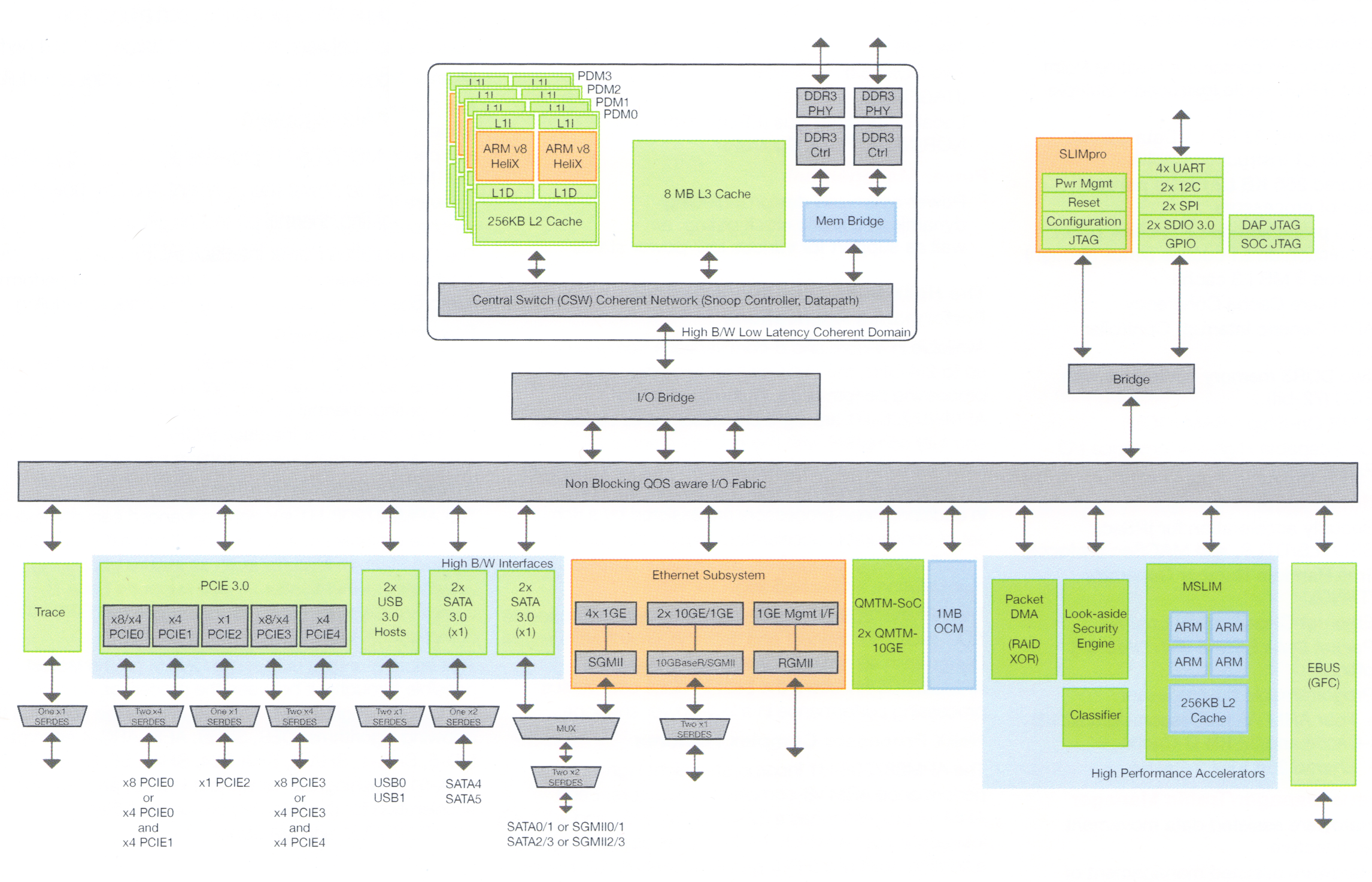
Applied Micro Helix Block Diagram
| Applied Micro HeliX Family | ||||
| APM887208-H1 | APM887104-H2 | |||
| Cores | 4 or 8 ARMv8 HeliX 1 at up to 2.4 GHz | 2 or 4 ARMv8 HeliX 2 at up to 2.0 GHz | ||
| L1 Cache | 32 KB I / 32 KB D per core (write-through with parity protection) | |||
| L2 Cache | 256 KB shared per core pair (with ECC) 64 | |||
| L3 Cache | 4 or 8 MB shared | 2 MB shared | ||
| DRAM | 2x DDR3 Controllers with ECC (72b each) | 1x DDR3 Controller with ECC (72b) | ||
| On-Chip Memory | 1 MB | 256 KB | ||
| Memory Bus Width | 256-bit | 256-bit | ||
| Low Power Features | N/A | < 250 mW standby | ||
| Coprocessors | 4x Cortex-A5 at 500 MHz | N/A | ||
| High-Speed Interfaces | 2x 10G + 4x 1G + 1x 1G Management Ethernet | 1x 10G + 4x 1G Ethernet | ||
| 17x PCIe 3.0 (2 x8 + 1 x1 OR 1 x8 + 2 x4 + 1 x1 OR 4 x4 + 1 x1) | 3x PCIe 3.0 (2 x1 OR 1 x4) | |||
|
|
2x USB 3.0 Host + 1x USB 3.0 Host/Device | |||
| 6x SATA III (four muxed with 4x 1G Ethernet) | 1x SATA III | |||
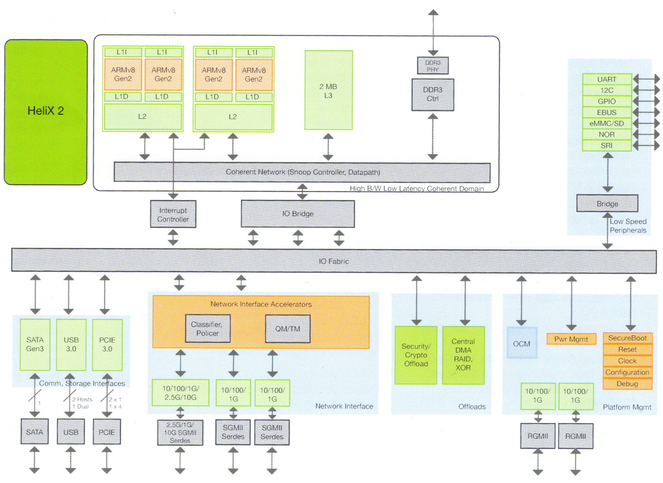
Applied Micro Helix 2 Block Diagram
The HeliX SoCs are sampling right now and slated to go into volume production in 2015. Applied Micro claims that design wins are already in place. From ARM's perspective, one can say that the juggernaut rolls on. With Cavium's Project Thunder and Broadcom's Vulcan targeting the high-end enterprise and datacenter segment, ARM needed an entry in the mid- to high-end embedded space currently dominated by MIPS64 and x86-64. The Applied Micro HeliX family brings ARM forward as a credible competitor for those sockets.
Source: Applied Micro


12 Comments
View All Comments
ZeDestructor - Friday, October 3, 2014 - link
The big chip with 6x SATA ports could make for an interesting low-power ZFS box... It even has ECC!Drizzt321 - Friday, October 3, 2014 - link
Yes indeed, plus a large number of PCIe slots available for more HBA cards. Or just for straight PCIe SSD card(s). Plus 2 DDR3 controllers (which is how many slots?), which means probably a decent amount of max memory.Although the part that it's muxed with the 4x1Gb Ethernet ports is concerning, but just don't use those ports since it appears there's a 1x10Gb and a 1x1Gb that aren't hooked up to the mux.
The other thing the PCIe slots allows is Thunderbolt, or for more enterprise settings Inifiband or the like.
tuxRoller - Sunday, October 5, 2014 - link
Maybe, but only if it has neon(which I think all armv8 do) and zfs makes use of it. Otherwise, you'd be doing compression and parity calcs on a fairly slow CPU.jospoortvliet - Tuesday, October 7, 2014 - link
Neon is an intricate part of ARMv8 so it sure is there. No idea if ZFS uses it but why not...ZeDestructor - Friday, October 3, 2014 - link
Ganesh: There's an error in your table: the APM887208-H1 has 2 USB3.0 host, not 1, according to the diagram.ganeshts - Friday, October 3, 2014 - link
I see what you are saying, but APM's datasheet is confusing in itself. The text documentation only indicates one USB 3.0 host with integrated PHY, but the block diagram indicates two USB 3.0 ports.milli - Friday, October 3, 2014 - link
I guess the diagrams were made by different people or something.I think both have one USB 3.0 controller which offers two ports.
ganeshts - Friday, October 3, 2014 - link
I got official confirmation from APM that the block diagram is right, but the text in their datasheet was wrong. I have fixed the table.azazel1024 - Friday, October 3, 2014 - link
What is odd to me is that Helix2 is the newer/smaller node, but much "smaller" chip in terms of core count and features, which means that Helix1 is probably a HUGE leap in power consumption being a full node larger and being a much more feature rich chip.dave1231 - Monday, October 6, 2014 - link
ARM could become the biggest company in the world if they continue like this. What a model. Even the LITTLE CPUS can be used in cheaper smartphones like the Desire 810. What can Intel do with all its money without licensing?