NVIDIA Announces Tegra 4i, Formerly Project Grey, With Integrated LTE and Phoenix Reference Design
by Brian Klug & Anand Lal Shimpi on February 19, 2013 9:00 AM ESTIt has been a while since we’ve heard anything about Project Grey, the first NVIDIA SoC with an integrated digital baseband, and the result of NVIDIA’s acquisition of soft-modem manufacturer Icera. Today, NVIDIA is ready to formalize Project Grey as Tegra 4i, and we have a bunch of information about this SoC and will obtain even more before MWC is upon us. NVIDIA’s roadmap from late 2011 put Grey in early 2013, and while other members of that roadmap haven’t necessarily stuck to the promised release schedule, Grey seems to be somewhere close to that schedule, at least as far as announcement and samples are concerned.
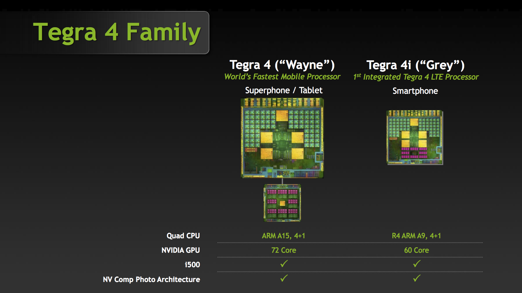
First, Tegra 4i includes the familiar 4+1 arrangement of cores we've seen since Tegra 3, but instead of Tegra 4's A15s, 4i includes ARM Cortex A9 CPUs running at a maximum single core clock of 2.3 GHz, we’re still waiting on a breakdown of the clock rates for dual and quad configuration, as well as the shadow core. NVIDIA has noted that it using R4 of ARM’s Cortex A9, which includes higher IPC thanks to the addition of a better data prefetching engine, dedicated hardware for cache preload instructions and some larger buffers. NVIDIA believes it is the first to implement the latest version of ARM's Cortex A9 core, however there's nothing stopping others from doing the same.
NVIDIA likely chose to integrate ARM's Cortex A9 r4 instead of the Cortex A15 to reduce power consumption and die size. While Tegra 4 is expected to be around 80mm^2, Tegra 4i measures in at around 60mm^2 including integrated baseband. NVIDIA isn't talking about memory interfaces at this point, but do keep in mind that your memory interface is often defined by the size of your die.

The 4i SoC is also built on TSMC’s 28 HPM process, interestingly enough not the 28 HPL process used for Tegra 4. As Tegra 4i appears to be geared towards hitting very high clock speeds, the use of TSMC's 28nm HPM process makes sense.
Tegra 4i also gets the exact same ISP and computational photography features that Tegra 4 includes, along with the same video encode and decode blocks. When it comes to the GPU side, 4i includes 60 GPU cores, that's just shy of the 72 in Tegra 4 proper. We’re waiting on additional detail to understand if these cores include the same enhancements we saw in Tegra 4 vs. Tegra 3. We also don't know the clock speed of the GPU cores in Tegra 4i.
| Tegra 4 Comparison | |||||||
| Tegra 4 | Tegra 4i | ||||||
| CPU Configuration | 4+1 ARM Cortex A15 | 4+1 ARM Cortex A9 "r4" | |||||
| Single CPU Max Clock | 1.9 GHz | 2.3 GHz | |||||
| Process | 28nm HPL | 28nm HPM | |||||
| GPU Cores | 72 | 60 | |||||
| Memory Interface | PCDDR3 and LPDDR3 | LPDDR3 | |||||
| Display | 3200x2000 | 1920x1200 | |||||
| Baseband | No Integrated Modem |
Icera i500 |
|||||
| Package |
23x23 BGA 14x14 FCCSP |
12x12 POP 12x12 FCCSP |
|||||
Tegra 4i also includes the Icera i500 baseband IP block on-die, hence i for Icera. NVIDIA has disclosed some additional detail about i500 along the lines of what we’ve already written about. There’s full support for Category 3 (100 Mbps) LTE at launch, with a later upgrade to Category 4, along with support for 10 MHz + 10 MHz LTE carrier aggregation. In addition there’s support for the rest of the 3GPP suite of air interfaces, including WCDMA / HSPA+ up to 42 Mbps (Category 24), TD-SCDMA, and GSM/EDGE. i500 is also voice enabled with VoLTE support and CS-FB voice modes. NVIDIA claims that the i500 package is 7x7mm with a 6.5x6.5mm transceiver, and there are a total of 8 primary Rx ports (bands). NVIDIA also claims support for both 2x2 MIMO and 4x4 MIMO transmission modes on LTE.
Functionally Tegra 4i is more like a heavily upgraded Tegra 3 than a Tegra 4 part thanks to the Cortex A9s. It's clear that Tegra 4i is aimed more at the smartphone market while Tegra 4 proper aims at tablets or other platforms with a higher power budget and greater performance demands.
In terms of time frame, NVIDIA expects the first Tegra 4i designs to begin shipping at the end of 2013, with most devices appearing in Q1 of 2014. It'll be interesting to see how a Cortex A9 based design holds up in Q1 2014, although the newer core and very high clock speed should do a good job of keeping the SoC feeling more modern than you'd otherwise expect.
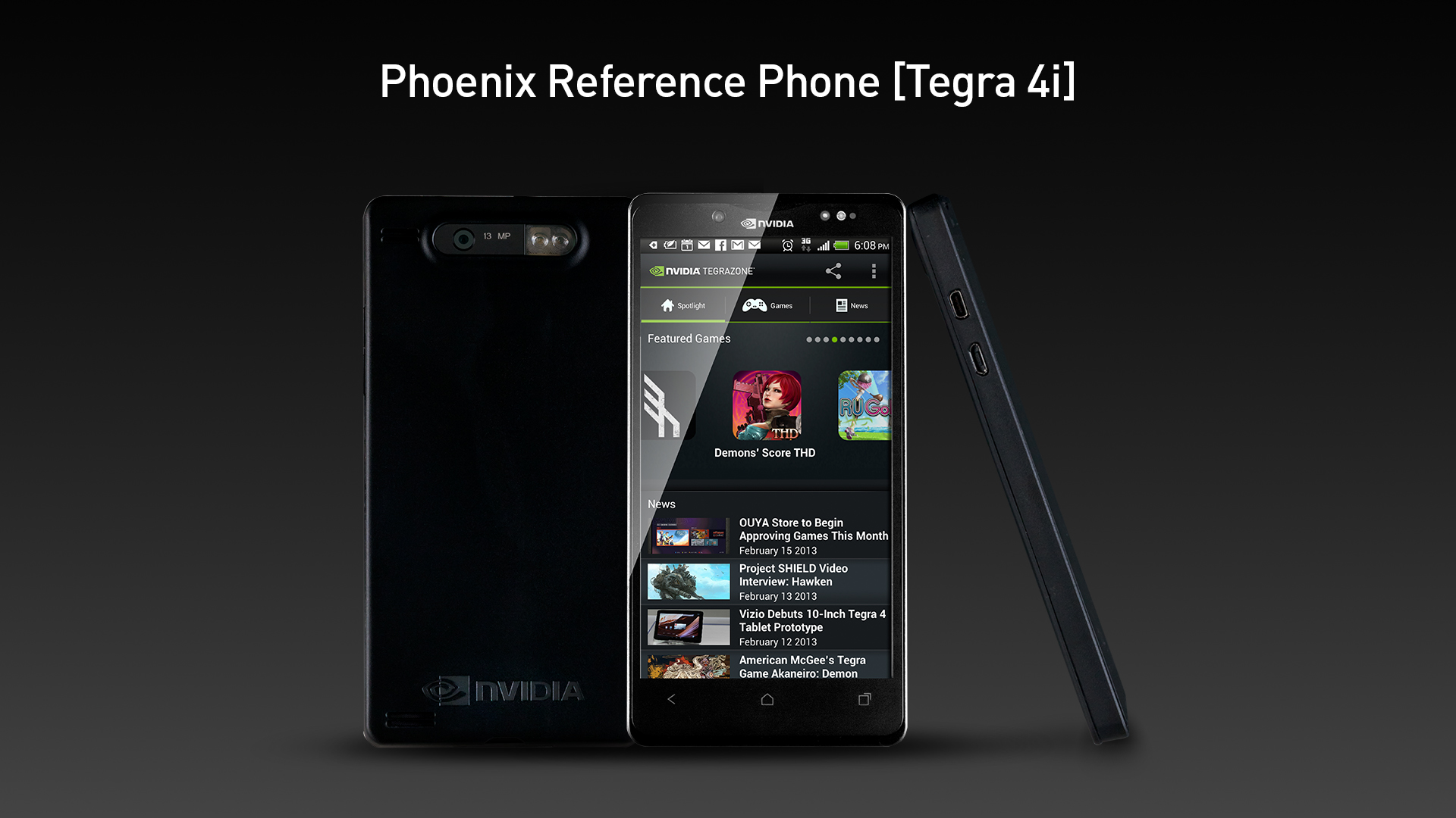
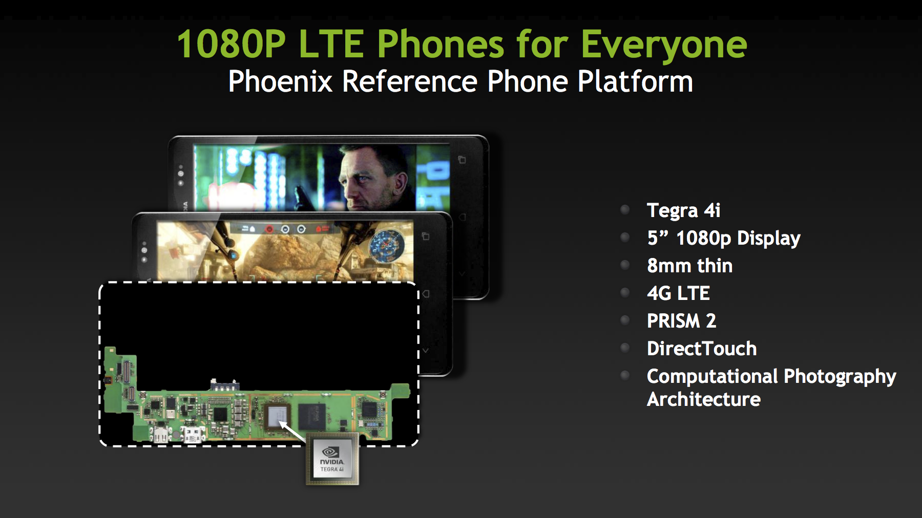
The other big announcement is a reference design built around Tegra 4i called Phoenix. It's a smartphone with Tegra 4i inside, 5-inch 1080p display, LTE, and just 8 mm of thickness. What's more impressive is that NVIDIA claims the reference design can be picked up by an OEM and ship with an unsubsidized price tag of between $100-$300 USD. With Phoenix NVIDIA now joins the likes of Qualcomm and Intel, both of whom already have active smartphone reference design programs.
We have a lot more questions about Tegra 4, 4i, and Phoenix, but answers are coming.


21 Comments
View All Comments
bleekii - Tuesday, February 19, 2013 - link
The Tegra 4i should be almost 26% larger to be at scale. The Tegra 4 is about 284px squared, and the Tegra 4i is only about 195px squared. It should be about 246px squared.284^2 is 80656
246^2 is 60516
Which is nearly proportional to 80mm^2 vs 60mm^2
djgandy - Thursday, February 21, 2013 - link
Tegra 4i is not going to be 60mm2 unless it is die shrunk or on some process that has far superior logic density. Get hi-res die shots of T4 and T4i and put them through image comparison. The layouts are almost identical!Note how much smaller the GPU ALU's are on the scaled down T4i die from the nvidia marketing slide.
mayankleoboy1 - Tuesday, February 19, 2013 - link
I see this as a desperate act by Nvidia. Their T4 design lacks a baseband, and uses quite a lot of power for a smartphone chip.So they use the old A9 arch, which cant be competitive with the A15 archs, even with a higher speed bump. And no "hundreds of design wins" , eh Jen-Hsun-Husang ?
I guess OEM's got tired of you
tviceman - Tuesday, February 19, 2013 - link
Please leave the flame baiting and fanboyism to mommy's basement.mayankleoboy1 - Tuesday, February 19, 2013 - link
As if Nvidia was a towering success with Tegrs2 and Tegra3..And Tegra4 has no OEM partners as of now. Only HP, which itself has been a towering failure in the mobile space.
andrewaggb - Tuesday, February 19, 2013 - link
He might be right though. Charlie at semiaccurate certainly seems to think tegra 4 is in trouble.Tegra 2/3 underwhelmed. Maybe tegra4 will as well.
andrewaggb - Tuesday, February 19, 2013 - link
I'm hoping it's good though. If the only players are apple, qualcomm, and samsung, it's not much of a market.tviceman - Tuesday, February 19, 2013 - link
In what ways did Tegra 2 and 3 underwhelm? Tegra powered more android tablets than any other vendor's SoC. If anything, the general sales of Android tablets have underwhelmed.Death666Angel - Tuesday, February 19, 2013 - link
Maybe those sale numbers weren't very high because people were disappointed with the Tegra2 performance in all those tablets? Just because it is in a lot of them (courtesy of Google using it as the dev platform for Honeycomb) doesn't mean it was actually a good SoC.Tegra2 sucked. It came too late and when it came it was underwhelming performance/power wise. Tegra3 was okay though. But it's been around for long enough.
I'll hold off commenting on T4(i) until I see Anand's review of it. Very interested in it though.
andrewaggb - Tuesday, February 19, 2013 - link
Personally I thought tegra 2 was very slow. Android tablets running tegra 2 felt horrible compared to the ipad. Some of it was android related, but regardless it wasn't good.Tegra 3 still had single channel memory and mid range gpu performance. It's not awful, but I still think Qualcomm and Apple had better SOC's.