TSMC: We Want OSATs to Expand Their Advanced Packaging Capability
by Anton Shilov on October 16, 2023 10:30 AM EST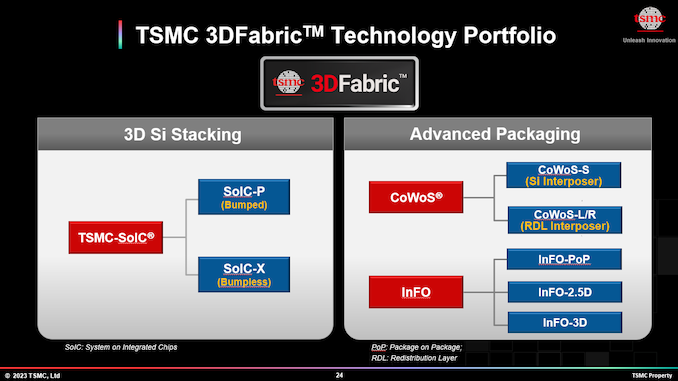
Almost since the inception of the foundry business model in the late 1980s, TSMC would produce silicon. In contrast, an outsourced semiconductor assembly and test (OSAT) service provider would then package it into a ceramic or organic encasing. Things have changed in recent years with the emergence of advanced packaging methods that require sophisticated tools and cleanrooms that are akin to those used for silicon production because TSMC was at the forefront of innovative packaging methods, which the company aggregates under the 3DFabric brand and because it built appropriate capacity, it quickly emerged as a significant OSAT for advanced packaging.
Many companies, such as Nvidia, want to send in blueprints and get their product that is ready to ship, which is why they choose to use TSMC's services to package their advanced system-in-packages, such as H100, using such technologies as integrated fan-out (InFO, chip first) and chip-on-wafer-on-substrate (CoWoS, chip last) developed by the foundry. As a result, TSMC had to admit earlier this year that it could not keep up with CoWoS demand and would expand appropriate production capacity.
Although TSMC makes tons of money on advanced chip packaging methods these days, the company does not have plans to steal business away from its traditional OSAT partners, which is why it wants these companies to expand their sophisticated packaging capacity and use similar tools to TSMC and its partners to offer to package compatible with TSMC-made chiplets.
But it is not that simple. All leading assembly and test specialists like ASE Group, Amkor Technology, and JCET have advanced chip packaging technologies, many resembling those of TSMC. These OSATs own advanced packaging fabs already and can serve fabless chip designers. For example, just this week, Amkor opened up its $1.6 billion advanced packaging facility in Vietnam. It is set to have a cleanroom space comparable to that GlobalFoundries owns across multiple fabs.
But while packaging technologies offered by OSATs may be similar to those of TSMC in terms of pitch dimensions and bump I/O pitch dimensions, they are not the same in terms of flow and may even have slightly different electric specifications. Meanwhile, OSATs use the same tools as TSMC, so they can pack chips that use CoWoS interposer. So far, TSMC has certified two OSATs to perform the final CoWoS assembly. However, there is still a shortage of CoWoS capacity on the market because TSMC's capacity is the bottleneck, at least based on TSMC's comments from earlier this year.
"So, we have ASE and SPIL, we have qualified their substrates," said Dan Kochpatcharin, Head of Design Infrastructure Management at TSMC, at the OIP 2023 conference in Amsterdam. "The next step is also doing the same thing to bring them into using the automated routing of the substrate as well. So, we can have the whole [CoWoS service] stack."
TSMC's advanced packaging technologies like CoWoS and InFO are supported by electronic design automation (EDA) tools from companies like Ansys, Cadence, Siemens EDA, and Synopsys. So, TSMC needs OSATs to use the same programs and align their technical capabilities with what these tools design and TSMC produces.
"We want them to use the same EDA tools," said Kochpatcharin. "So, let's say TSMC interposer on OSAT's substrate. So, they use 3Dblox and [appropriate] EDA tools to do analysis, then it is easier for the customer. Right? Like we qualified the two partners to [produce] substrate. So, we do CoWoS, and OSATs do substrate. So, it would be good to use the same flow, because it is easier for customer. "If you have customers who use [different EDA tools] then the multi physics analysis [of the package] will be more difficult. It can be done just more difficult."
To meet the demand for CoWoS and other advanced packaging methods, OSATs need to invest in appropriate capacities and tools, which are expensive. The problem is that assembly and test specialists cannot keep up with Intel, TSMC, and Samsung regarding investments in advanced packaging facilities. Last year, Intel spent $4 billion on advanced packaging plants, and TSMC's capital expenditures on advanced packaging totaled $3.6 billion. In contrast, Samsung spent around $2 billion, according to Yole Group's estimates published by EE Times. By comparison, the capital expenditures of ASE Group (with SPIL and USI) totaled $1.7 billion in 2022, whereas the spending of Amkor reached $908 million.
There are several reasons why advanced packaging technologies like TSMC's CoWoS and InFO, as well as Intel's EMIB and Foveros, are gaining importance. First up, disaggregated chip designs are getting more popular because chip manufacturing is getting more expensive, smaller chips are easier to yield, and many chips are reaching the reticle limit. At the same time, their designers want them to be bigger and more powerful. Secondly, disaggregated designs using chiplets made on different nodes are cheaper than one monolithic chip on a leading-edge node.
OSATs are poised to expand their advanced production capacities as their clients demand appropriate services. Meanwhile, they are less inclined to offer such services than foundries simply because if something fails during packaging steps, they have to throw away all the expensive silicon they package, and they do not earn as much as chipmakers do. Their margins are also significantly lower. Finally, it may be unclear in many cases why a multi-chiplet package does not work and whether the problem is with the package itself or with one of the chips. Today, all TSMC can do is to optically check the wafers before dicing them, but this is not a particularly efficient way of testing.
To gain the capability to test chiplets individually, TSMC is working with makers of chip test equipment and expects to validate these tools next year.
"On the 3DFabric on the testing, we work with Advantest, Teradyne, and Synopsys to leverage the high-speed die-to-die testing," said Kochpatcharin. "When you have all these things stacked together, it is getting very difficult to test them. So, we have worked with Teradyne and Advantest to work […] [die-to-die] testing, and we will have silicon validation in 2024."


2 Comments
View All Comments
Threska - Tuesday, October 17, 2023 - link
"There are several reasons why advanced packaging technologies like TSMC's CoWoS and InFO, as well as Intel's EMIB and Foveros, are gaining importance."One can also do a more tailored design as well. e.g. mixed analog/digital, etc.
PackagingGuru - Tuesday, October 17, 2023 - link
OSATs have the capabilities as mentioned in the article, with the exception of wafer-to-wafer bonding, which is not really needed unless you are stacking memory or specialty wafers. The abilities for both traditional and advanced packaging capabilities are much more extensive in the OSATs and will continue to add value as the heterogeneous integration design strategy expands. TSMC has the leadership position because of 1 main reason- they want to sell their next generation silicon node wafers at very high prices and by offering the advanced packaging with this, they are able to lock their customers in. With Samsung and Intel offering adv. nodes as well, more companies will be looking to leverage on "open source" network of advanced packaging suppliers and the OSAT's have the edge with the broad range of packaging tools at their disposal for system level integration.