Micron Unveils HBM3 Gen2 Memory: 1.2 TB/sec Memory Stacks For HPC and AI Processors
by Anton Shilov on July 26, 2023 9:00 AM EST
Micron today is introducing its first HBM3 memory products, becoming the latest of the major memory manufacturers to start building the high bandwidth memory that's widely used in server-grade GPUs and other high-end processors. Aiming to make up for lost time against its Korean rivals, Micron intends to essentially skip "vanilla" HBM3 and move straight on to even higher bandwidth versions of the memory they're dubbing "HBM3 Gen2", developing 24 GB stacks that run at over 9 GigaTransfers-per-second. These new HBM3 memory stacks from Micron will target primarily AI and HPC datacenter, with mass production kicking off for Micron in early 2024.
Micron's 24 GB HBM3 Gen2 modules are based on stacking eight 24Gbit memory dies made using the company's 1β (1-beta) fabrication process. Notably, Micron is the first of the memory vendors to announce plans to build HBM3 memory with these higher-density dies, while SK hynix offers their own 24 GB stacks, the company is using a 12-Hi configuration of 16Gbit dies. So Micron is on track to be the first vendor to offer 24 GB HBM3 modules in the more typical 8-Hi configuration. And Micron is not going to stop at 8-Hi 24Gbit-based HBM3 Gen2 modules, either, with the company saying that they plan to introduce even higher capacity class-leading 36 GB 12-Hi HBM3 Gen2 stacks next year.
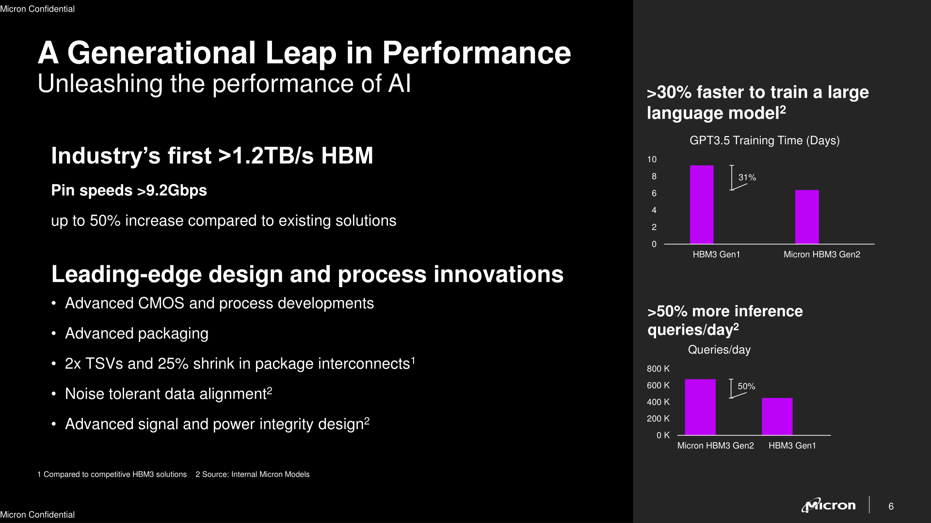
Besides taking the lead in density, Micron is also looking to take a lead in speed. The company expects its HBM3 Gen2 parts to hit date rates as high as 9.2 GT/second, 44% higher than the top speed grade of the base HBM3 specification, and 15% faster than the 8 GT/second target for SK hynix's rival HBM3E memory. The increased data transfer rate enables each 24 GB memory module to offer peak bandwidth of 1.2 TB/sec per stack.
Micron says that 24GB HBM3 Gen2 stacks will enable 4096-bit HBM3 memory subsystems with a bandwidth of 4.8 TB/s and 6096-bit HBM3 memory subsystems with a bandwidth of 7.2 TB/s. To put the numbers into context, Nvidia's H100 SXM features a peak memory bandwidth of 3.35 TB/s.
| HBM Memory Comparison | ||||||
| "HBM3 Gen2" | HBM3 | HBM2E | HBM2 | |||
| Max Capacity | 24 GB | 24 GB | 16 GB | 8 GB | ||
| Max Bandwidth Per Pin | 9.2 GT/s | 6.4 GT/s | 3.6 GT/s | 2.0 GT/s | ||
| Number of DRAM ICs per Stack | 8 | 12 | 8 | 8 | ||
| Effective Bus Width | 1024-bit | |||||
| Voltage | 1.1 V? | 1.1 V | 1.2 V | 1.2 V | ||
| Bandwidth per Stack | 1.2 TB/s | 819.2 GB/s | 460.8 GB/s | 256 GB/s | ||
High frequencies aside, Micron's HBM3 Gen2 stacks are otherwise drop-in compatible with current HBM3-compliant applications (e.g., compute GPUs, CPUs, FPGAs, accelerators). So device manufacturers will finally have the option of tapping Micron as an HBM3 memory supplier as well, pending the usual qualification checks.
Under the hood, Micron's goal to jump into an immediate performance leadership position within the HBM3 market means that they need to one-up their competition from a technical level. Among other changes and innovations to accomplish that, the company increased the number of through-silicon vias (TSVs) by two times compared to shipping HBM3 products. In addition, Micron shrunk the distance between DRAM devices in its HBM3 Gen2 stacks. These two changes to packaging reduced thermal impendence of these memory modules and made it easier to cool them down. Yet, the increased number of TSVs can bring other advantages too.
Given that Micron uses 24 Gb memory devices (rather than 16 Gb memory devices) for its HBM3 Gen2 stacks, it is inevitable that it had to increase the number of TSVs to ensure proper connectivity. Yet, doubling the number of TSVs in an HBM stack can enhance overall bandwidth (and shrink latency), power efficiency, and scalability by facilitating more parallel data transfers. It also improves reliability by mitigating the impact of single TSV failures through data rerouting. However, these benefits come with challenges such as increased manufacturing complexity and increased potential for higher defect rates (already an ongoing concern for HBM), which can translate to higher costs.
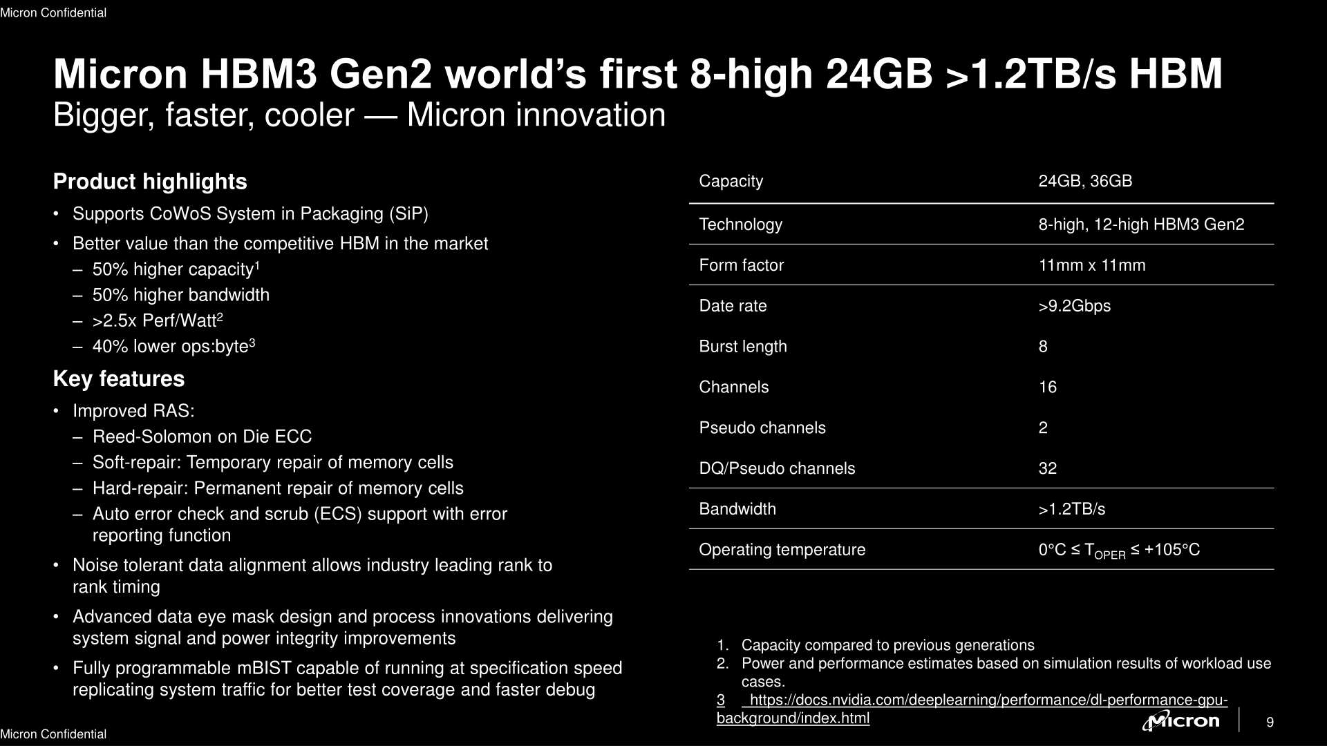
Just like other HBM3 memory modules, Micron's HBM3 Gen2 stacks feature Reed-Solomon on-die ECC, soft repair of memory cells, hard-repair of memory cells as well as auto error check and scrub support.
Micron says it will mass produce its 24 GB HBM3 modules starting in Q1 2024, and will start sampling its 12-Hi 36GB HBM3 stacks around this time as well. The latter will enter high volume production in the second half of 2024.
To date, the JEDEC has yet to approve a post-6.4GT/second HBM3 standard. So Micron's HBM3 Gen2 memory, as well as SK hynix's rival HBM3E memory, are both off-roadmap standards for the moment. Given the interest in higher bandwidth HBM memory and the need for standardization, we'd be surprised if the group didn't eventually release an updated version of the HBM3 standard that Micron's devices will conform to. Though as the group tends to shy away from naming battles ("HBM2E" was never a canonical product name for faster HBM2, despite its wide use), it's anyone's guess how this latest kerfuffle over naming will play out.
Beyond their forthcoming HBM3 Gen2 products, Micron is also making it known that the company already working on HBMNext (HBM4?) memory. That iteration of HBM will provide 1.5 TB/s – 2+ TB/s of bandwidth per stack with capacities ranging from 36 GB to 64 GB.


Source: Micron


7 Comments
View All Comments
meacupla - Wednesday, July 26, 2023 - link
oh man, if only all of this HBM wasn't being gobbled up by AI processors.24GB of HBM on a Z1 extreme/7840U would be amazing, if possible.
brucethemoose - Wednesday, July 26, 2023 - link
Even if ig was available, its just not economical, see https://semiengineering.com/hbms-future-necessary-...There is nothing stopping Intel/AMD from making higher bandwidth LPDDRX APUs, hence rumors suggest there will be quad channel Arrow Lake-generation APUs.
nandnandnand - Thursday, July 27, 2023 - link
I've heard about Strix Halo with its doubled memory bus, but not a quad-channel Arrow Lake APU. Got a link for it?Santoval - Wednesday, July 26, 2023 - link
“Micron says that 24GB HBM3 Gen2 stacks will enable 4096-bit HBM3 memory subsystems with a bandwidth of 4.8 TB/s and 6096-bit HBM3 memory subsystems with a bandwidth of 7.2 TB/s..”Since they doubled the TSVs I assume they should be able to support up to a 8,192-bit bus eventually, right? Maybe a few hundred bits less to account for bad TSVs in some wafers.
andychow - Tuesday, August 8, 2023 - link
I don't think so. It means they doubled the die stacks, but the bus width is likely up to the controller.Shmee - Thursday, July 27, 2023 - link
This should go on video cards. Could go great on the next RDNA, along with the chiplet design.parrot1553 - Tuesday, August 1, 2023 - link
the 7900XTX already has over 1TB/s bandwidth, so not really impressive at all.