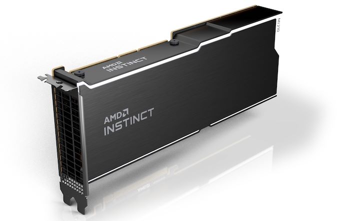
AMD Releases Instinct MI210 Accelerator: CDNA 2 On a PCIe Card
by Ryan Smith on March 22, 2022 9:00 AM EST- Posted in
- GPUs
- AMD
- HPC
- AMD Instinct
- Infinity Fabric
- CDNA 2
With both GDC and GTC going on this week, this is a big time for GPUs of all sorts. And today, AMD wants to get in on the game as well, with the release of the PCIe version of their MI200 accelerator family, the MI210.
First unveiled alongside the MI250 and MI250X back in November, when AMD initially launched the Instinct MI200 family, the MI210 is the third and final member of AMD’s latest generation of GPU-based accelerators. Bringing the CDNA 2 architecture into a PCIe card, the MI210 is being aimed at customers who are after the MI200 family’s HPC and machine learning performance, but need it in a standardized form factor for mainstream servers. Overall, the MI200 is being launched widely today as part of AMD moving the entire MI200 product stack to general availability for OEM customers.
| AMD Instinct Accelerators | ||||||
| MI250 | MI210 | MI100 | MI50 | |||
| Compute Units | 2 x 10⁴ | 104 | 120 | 60 | ||
| Matrix Cores | 2 x 416 | 416 | 480 | N/A | ||
| Boost Clock | 1700MHz | 1700MHz | 1502MHz | 1725MHz | ||
| FP64 Vector | 45.3 TFLOPS | 22.6 TFLOPS | 11.5 TFLOPS | 6.6 TFLOPS | ||
| FP32 Vector | 45.3 TFLOPS | 22.6 TFLOPS | 23.1 TFLOPS | 13.3 TFLOPS | ||
| FP64 Matrix | 90.5 TFLOPS | 45.3 TFLOPS | 11.5 TFLOPS | 6.6 TFLOPS | ||
| FP32 Matrix | 90.5 TFLOPS | 45.3 TFLOPS | 46.1 TFLOPS | 13.3 TFLOPS | ||
| FP16 Matrix | 362 TFLOPS | 181 TFLOPS | 184.6 TFLOPS | 26.5 TFLOPS | ||
| INT8 Matrix | 362.1 TOPS | 181 TOPS | 184.6 TOPS | N/A | ||
| Memory Clock | 3.2 Gbps HBM2E | 3.2 Gbps HBM2E | 2.4 Gbps HBM2 | 2.0 Gbps GDDR6 | ||
| Memory Bus Width | 8192-bit | 4096-bit | 4096-bit | 4096-bit | ||
| Memory Bandwidth | 3.2TBps | 1.6TBps | 1.23TBps | 1.02TBps | ||
| VRAM | 128GB | 64GB | 32GB | 16GB | ||
| ECC | Yes (Full) | Yes (Full) | Yes (Full) | Yes (Full) | ||
| Infinity Fabric Links | 6 | 3 | 3 | N/A | ||
| CPU Coherency | No | N/A | N/A | N/A | ||
| TDP | 560W | 300W | 300W | 300W | ||
| Manufacturing Process | TSMC N6 | TSMC N6 | TSMC 7nm | TSMC 7nm | ||
| Transistor Count | 2 x 29.1B | 29.1B | 25.6B | 13.2B | ||
| Architecture | CDNA 2 | CDNA 2 | CDNA (1) | Vega | ||
| GPU | 2 x CDNA 2 GCD "Aldebaran" |
CDNA 2 GCD "Aldebaran" |
CDNA 1 "Arcturus" |
Vega 20 | ||
| Form Factor | OAM | PCIe (4.0) | PCIe (4.0) | PCIe (4.0) | ||
| Launch Date | 11/2021 | 03/2022 | 11/2020 | 11/2018 | ||
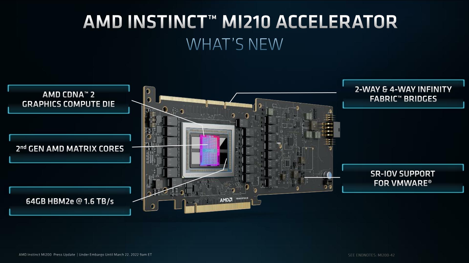
Starting with a look at the top-line specifications, the MI210 is an interesting variant to the existing MI250 accelerators. Whereas those two parts were based on a pair of Aldebaran (CDNA 2) dies in an MCM configuration on a single package, for MI210 AMD is paring everything back to a single die and related hardware. With MI250(X) requiring 560W in the OAM form factor, AMD essentially needed to halve the hardware anyhow to get things down to 300W for a PCIe card. So they’ve done so by ditching the second on-package die.
The net result is that the MI210 is essentially half of an MI250, both in regards to physical hardware and expected performance. The CNDA 2 Graphics Compute Die features the same 104 enabled CUs as on MI250, with the chip running at the same peak clockspeed of 1.7GHz. So workload scalability aside, the performance of the MI210 is for all practical purposes half of a MI250.
That halving goes for memory, as well. As MI250 paired 64GB of HBM2e memory with each GCD – for a total of 128GB of memory – MI210 brings that down to 64GB for the single GCD. AMD is using the same 3.2GHz HBM2e memory here, so the overall memory bandwidth for the chip is 1.6 TB/second.
In regards to performance, the use of a single Aldebaran die does make for some odd comparisons to AMD’s previous-generation PCIe card, the Radeon Instinct MI100. While clocked higher, the slightly reduced number of CUs relative to the MI100 means that for some workloads, the old accelerator is, at least on paper, a bit faster. In practice, MI210 has more memory and more memory bandwidth, so it should still have the performance edge the real world, but it’s going to be close. In workloads that can’t take advantage of CDNA 2’s architectural improvements, MI210 is not going to be a step up from MI100.
All of this underscores the overall similarity between the CDNA (1) and CDNA 2 architectures, and how developers need to make use of CDNA 2’s new features to get the most out of the hardware. Where CDNA 2 shines in comparison to CDNA (1) is with FP64 vector workloads, FP64 matrix workloads, and packed FP32 vector workloads. All three use cases benefit from AMD doubling the width of their ALUs to a full 64-bits wide, allowing FP64 operations to be processed at full speed. Meanwhile, when FP32 operations are packed together to completely fill the wider ALU, then they too can benefit from the new ALUs.
But, as we noted in our initial MI250 discussion, like all packed instruction formats, packed FP32 isn’t free. Developers and libraries need to be coded to take advantage of it; packed operands need to be adjacent and aligned to even registers. For software being written specifically for the architecture (e.g. Frontier), this is easily enough done, but more portable software will need updated to take this into account. And it’s for that reason that AMD wisely still advertises its FP32 vector performance at full rate (22.6 TFLOPS), rather than assuming the use of packed instructions.
The launch of the MI210 also marks the introduction of AMD’s improved matrix cores into a PCIe card. For CDNA 2, they’ve been expanded to allow full-speed FP64 matrix operation, bringing them up to the same 256 FLOPS rate as FP32 matrix operations, a 4x improvement over the old 64 FLOPS/clock/CU rate.
| AMD GPU Throughput Rates (FLOPS/clock/CU) |
|||||
| CDNA 2 | CDNA (1) | Vega 20 | |||
| FP64 Vector | 128 | 64 | 64 | ||
| FP32 Vector | 128 | 128 | 128 | ||
| Packed FP32 Vector | 256 | N/A | N/A | ||
| FP64 Matrix | 256 | 64 | 64 | ||
| FP32 Matrix | 256 | 256 | 128 | ||
| FP16 Matrix | 1024 | 1024 | 256 | ||
| BF16 Matrix | 1024 | 512 | N/A | ||
| INT8 Matrix | 1024 | 1024 | N/A | ||
Moving on, the PCIe format MI210 also gets a trio of Infinity Fabric 3.0 links along the top of the card, just like the MI100. This allows an MI210 card to be linked up with one or three other cards, forming a 2 or 4-way cluster of cards. Meanwhile, backhaul to the CPU or any other PCIe devices is provided via a PCIe 4.0 x16 connection, which is being powered by one of the flexible IF links from the GCD.
As previously mentioned, the TDP for the MI210 is set at 300W, the same level as the MI100 and MI50 before it – and essentially the limit for a PCIe server card. Like most server accelerators, this is fully passive dual slot card design, relying on significant airflow from the server chassis to keep things cool. The GPU itself is powered by a combination of the PCIe slot and an 8 pin, EPS12V connector at the rear of the card.
Otherwise, despite the change in form factors, AMD is going after much the same market with MI210 as they have MI250(X). Which is to say HPC users who specifically need a fast FP64 accelerator. Thanks to its heritage as a chip designed first and foremost for supercomputers (i.e. Frontier), the MI200 family currently stands alone in its FP64 vector and FP64 matrix performance, as rival GPUs have focused instead on improving performance at the lower precisions used in most industry/non-scientific workloads. Though even at lower precisions, the MI200 family is nothing to sneeze at with tis 1024 FLOPS-per-CU rate on FP16 and BF16 matrix operations.
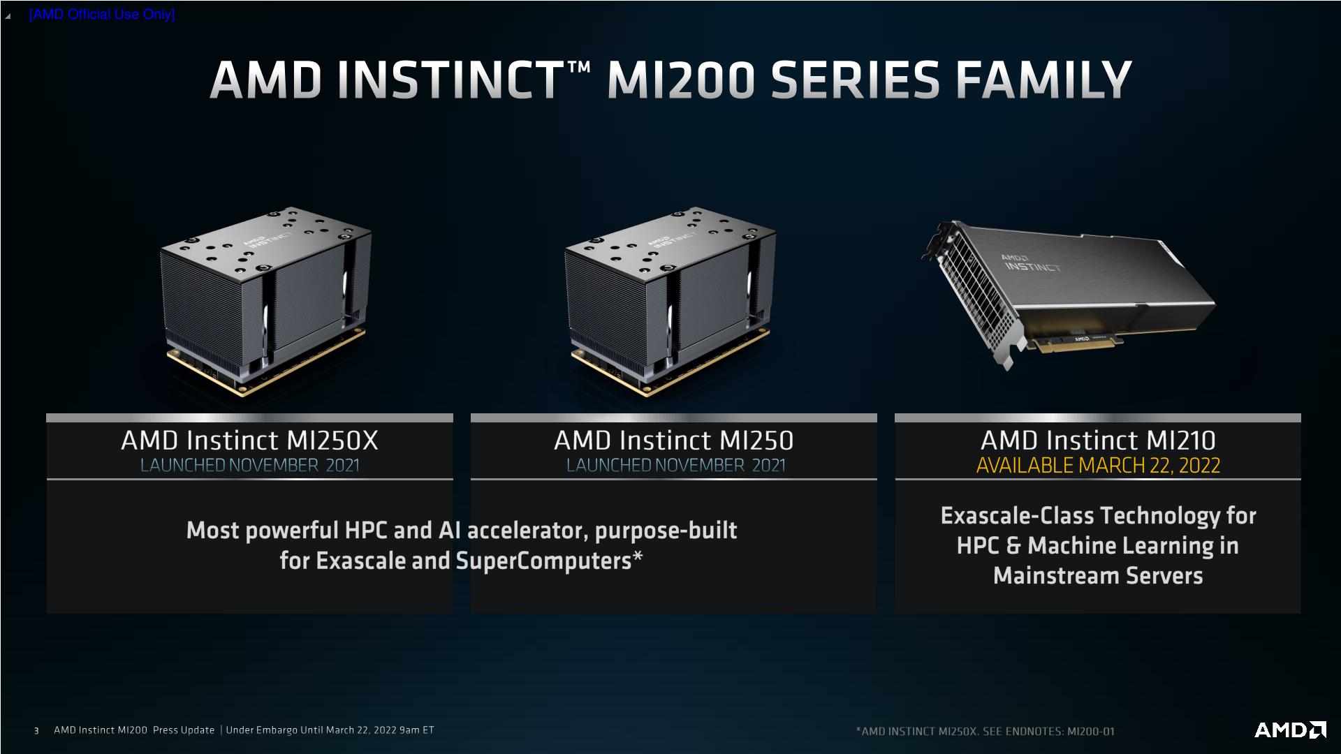
Wrapping things up, MI210 is slated to become available today from AMD’s usual server partners, including ASUS, Dell, Supermicro, HPE, and Lenovo. Those vendors are now also offering servers based on AMD’s MI250(X) accelerators, so AMD’s more mainstream customers will have access to systems based on AMD’s full lineup of MI200 accelerators.


39 Comments
View All Comments
nandnandnand - Tuesday, March 22, 2022 - link
Wake me up inside when I can get CDNA 5 in an M.2 module.https://www.cnx-software.com/2022/03/22/quadric-de...
mode_13h - Wednesday, March 23, 2022 - link
A good move would be to get these Matrix Cores in their RDNA-enabled APUs.As for M.2 as a compute accelerator form factor, I don't really see the point. Sure, it fits a SBC better than a big PCIe card, but most desktop PCs have enough PCIe slots and better cooling for PCIe cards to make more sense.
I think Quadric is late to the game, by offering a dedicated chip for edge AI processing at this stage. Most customers would probably opt for a SoC with an integrated AI engine. Maybe that's another option they're pursuing, but most SoC vendors already have their own AI engines.
Anyway, it'd be interesting to see some benchmarks of their stuff. I think it probably won't stack up too well against next-gen APUs equipped with tensor/matrix cores.
lemurbutton - Tuesday, March 22, 2022 - link
Boring. Wake me up when AMD can do transparent multi GPUs like M1 Ultra.mode_13h - Wednesday, March 23, 2022 - link
For HPC applications, there's less need to. That's mainly something you have to tackle for graphics, because graphics is much harder to neatly partition and involve more global data movement.So, my prediction is that the first AMD GPU to do that will probably be in their RDNA line, not CDNA.
PaulHoule - Friday, April 29, 2022 - link
Is that really true? There are big servers in HPC that have multiple GPUs. For instance the DGX-2https://www.nvidia.com/content/dam/en-zz/Solutions...
has 16 GPUs controlled by one CPU motherboard that has 2 Xeon sockets. I worked for a company that used a DGX-1 which had 8 GPU sockets and 2 CPU sockets and the system balance was just fine (with some thought about how to encode the training data) for training CNN neural networks
Spunjji - Thursday, March 24, 2022 - link
You'll be seeing that later this year - and unlike M1 Ultra, it will have good performance in the vast majority of apps people actually use.Of course none of this has any relevance to datacentre GPUs. You might be lost?
Unashamed_unoriginal_username_x86 - Wednesday, March 23, 2022 - link
Wake me up when september ends... It's march? Oh, uhhI'd be curious to see if servers with PCI-e accelerators could ever use tech like WBs with quick detach fittings and the new 12-pin power connector to reduce that huge power budget gap to mezzanine cards.
mode_13h - Wednesday, March 23, 2022 - link
Ryan, the MI100's GPU is codenamed Arcturus. It fits in with their stellar-based naming scheme and is plastered all over the Linux driver code.> packed FP32 isn’t free. ...packed operands need to be adjacent and aligned to even registers.
This is like how previous generations dealt with FP64. Your FP64 operands would be split across register pairs, or so I've heard.
The decision to stick with PCIe 4.0 seems a bit weird, since Genoa will presumably have PCIe 5.0 and there should be some considerable overlap in their respective product cycles. I guess AMD is figuring most of their big customers will use OAM form factor, with Infinity Link for CPU communication.
Anyway, AMD really needs to get some of these Matrix Cores into their RDNA product line, if they want the open source community to embrace them and broaden software support for them. Until then, I'm really not much interested. Regardless, my next dGPU will probably be Intel, due to AMD's poor track record of RDNA support for their compute stack.
Khanan - Wednesday, March 23, 2022 - link
“Anyway, AMD really needs to get some of these Matrix Cores into their RDNA product line, if they want the open source community to embrace them and broaden software support for them.”This isn’t relevant for server GPUs, nor are Matrix cores at this point relevant for gaming GPUs, simply buy a Instinct GPU then, if you want it.
“Regardless, my next dGPU will probably be Intel, due to AMD's poor track record of RDNA support for their compute stack.”
That’s pretty funny given the fact that intel so far hasn’t delivered any dGPUs and has proven nothing, probably a fan boy comment.
mode_13h - Thursday, March 24, 2022 - link
> nor are Matrix cores at this point relevant for gaming GPUsDon't agree. Maybe not fp64, but fp32 and lower-precision have applicability to games. At the lowest-precision, they can use it for AI-driven upscaling, like Nvidia's DLSS.
> simply buy a Instinct GPU then, if you want it.
How many developers have that kind of money? This is why Nvidia is winning the the GPU-compute race. Because they support development on their *entire* stack of GPUs, even down to the near-bottom tier of gaming GPUs and the Jetson development boards.
> That’s pretty funny given the fact that intel so far hasn’t delivered any dGPUs
They have a long track record with iGPUs. At my job, we use their iGPUs in a shipping product.
> probably a fan boy comment.
AMD can ignore these sentiments at its peril.