Samsung Teases 512 GB DDR5-7200 Modules
by Dr. Ian Cutress on August 22, 2021 1:02 PM EST
This week as part of the annual Hot Chips semiconductor conference, Samsung’s memory division has presented a poster/slides on a project it is currently working on with impressive end-point results. The company details a 512 GB module of DDR5 memory, running at DDR5-7200, designed for server and enterprise use. This is a step up from the 256 GB modules at the top end of the market today, but to get there, Samsung has been introducing some new features and functionality.
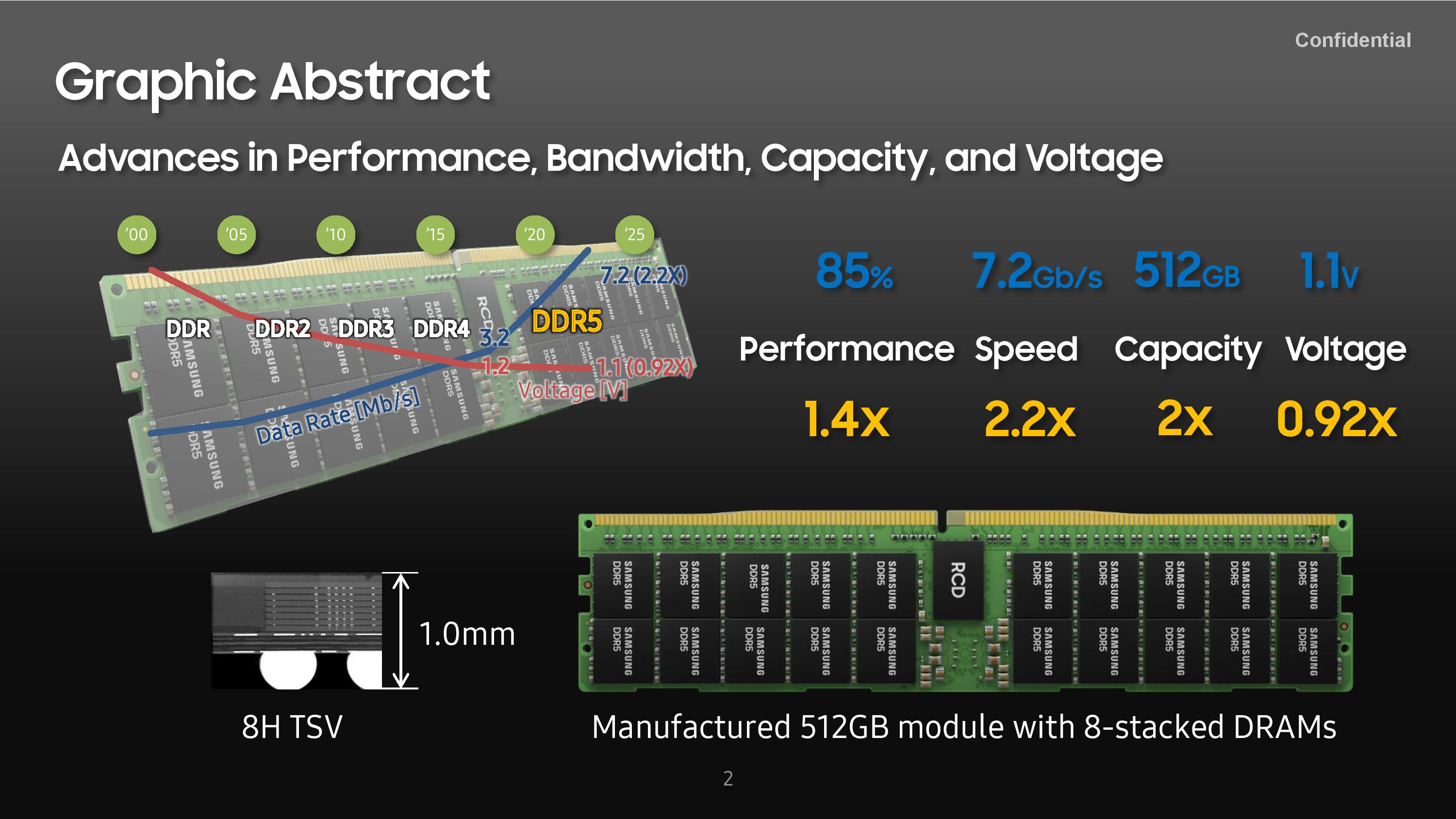
As per standard DDR5 specifications, the modules will run at 1.1 volts with standard JEDEC DDR5-7200 timings, however even JEDEC has not declared an official DDR5-7200 standard at this stage, choosing only to go to DDR5-6400. There are placeholders for future standards, such as DDR5-7200, and based on how the latencies increase from slower speed to higher speed, these should be in the realm of 50-50-50 to 60-60-60*.
*There are three variants for each DDR5 standard – A, B, or C.
DDR5-6400A is 46-46-46 for example, but
DDR5-6400C is 56-56-56.
As part of the presentation, Samsung states that the introduction of Same-Bank refresh (SBR) into its DDR5 will increase the efficiency of the DRAM bus connectivity by almost 10%, with DDR4-4800 showing the best efficiency in terms of energy from bit.

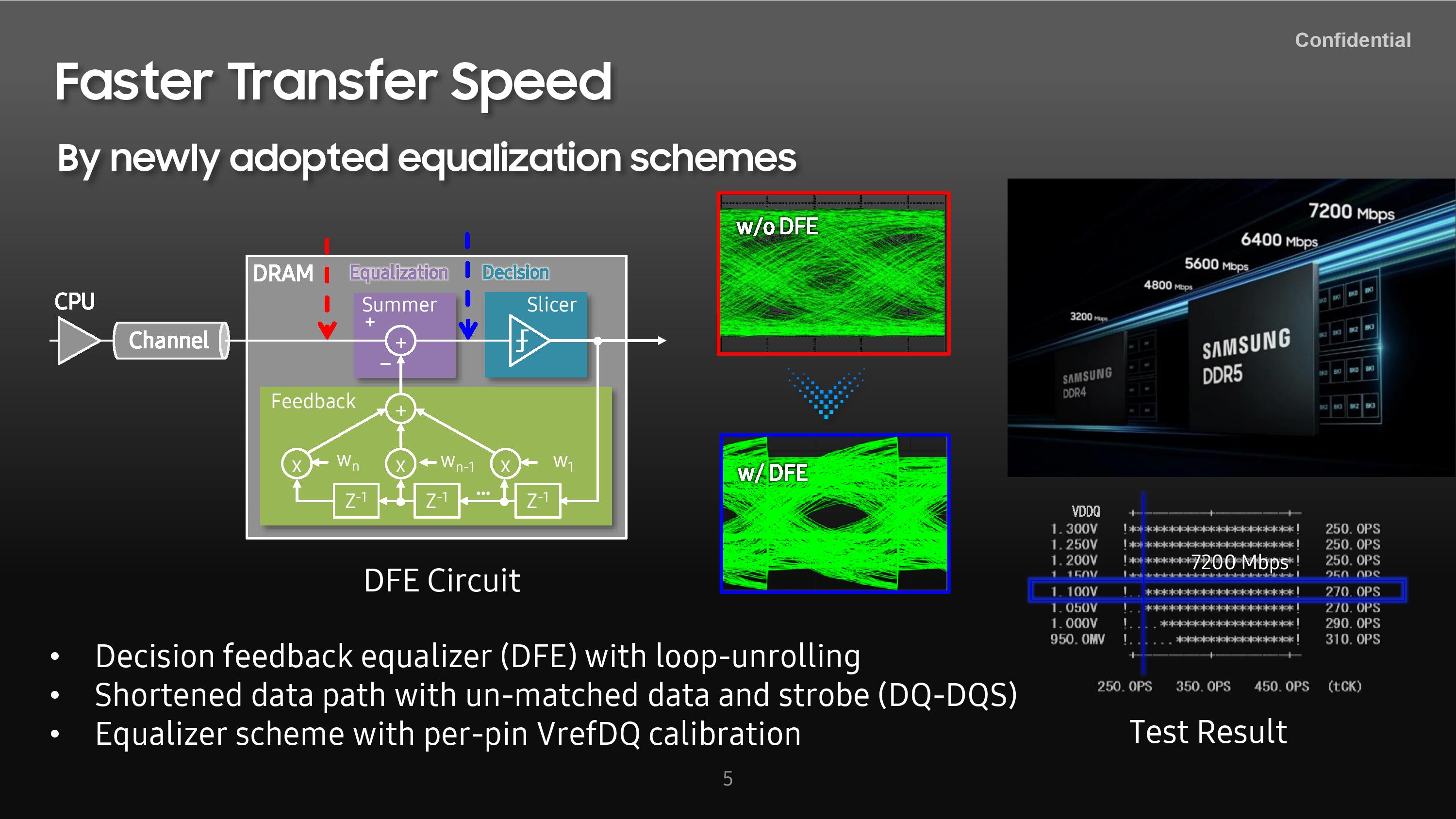
In order to support the higher memory transfer rates of DDR5, Samsung has introduced a new DFE (Decision Feedback Equalizer) for better signal stability. It allows for a more variable data-path location, as well as per-pin calibration techniques.
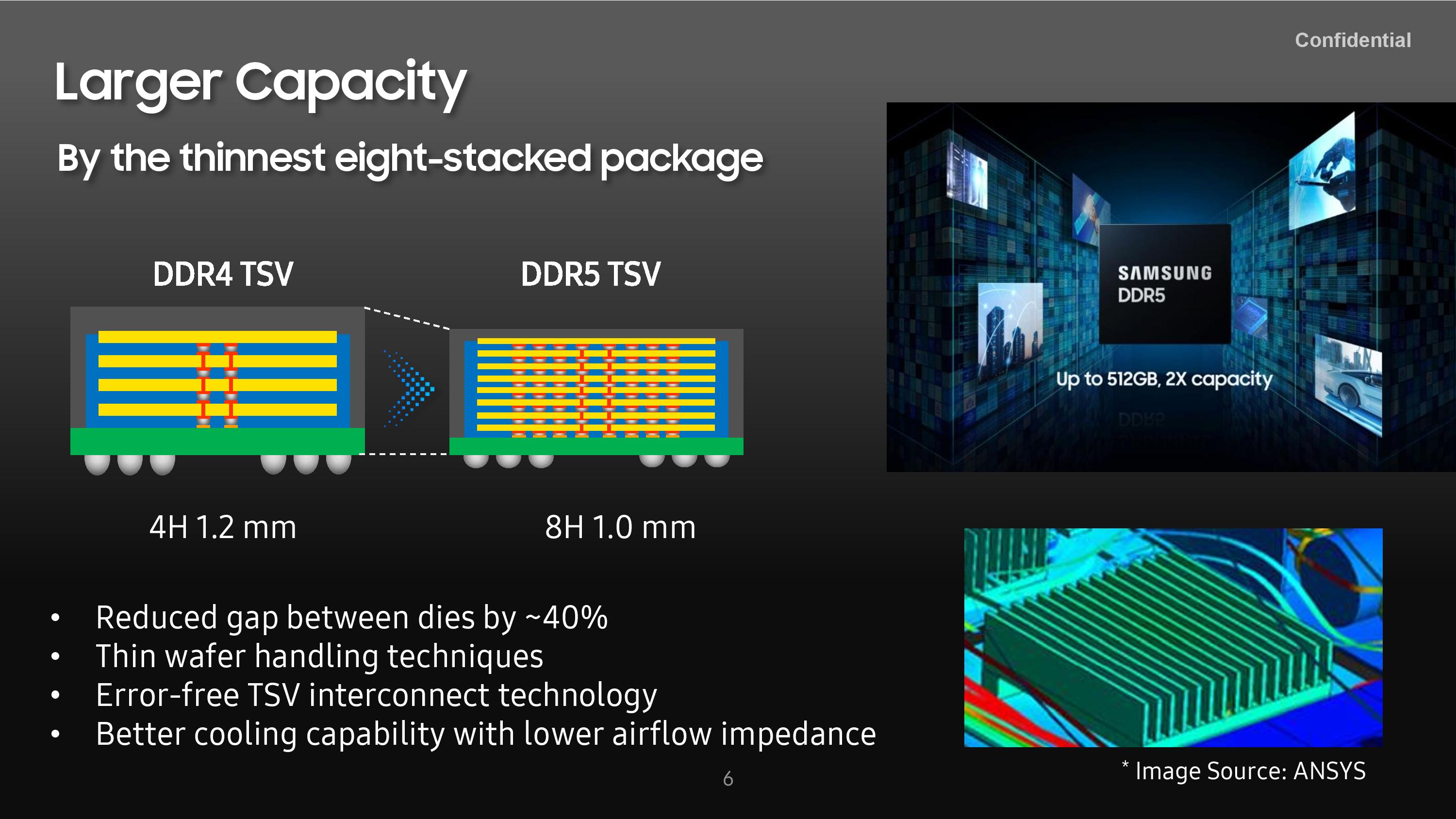
One of the big things about increasing capacity in memory is that you end up stacking more memory together. For their part, Samsung is stating that they can stack 8 DDR5 dies together and still be smaller than 4 dies of DDR4. This is achieved by thinning each die, but also new through-silicon-via connection topographies that allow for a reduced gap between dies of up to 40%. This is partnered by new cooling technologies between dies to assist with thermal performance.
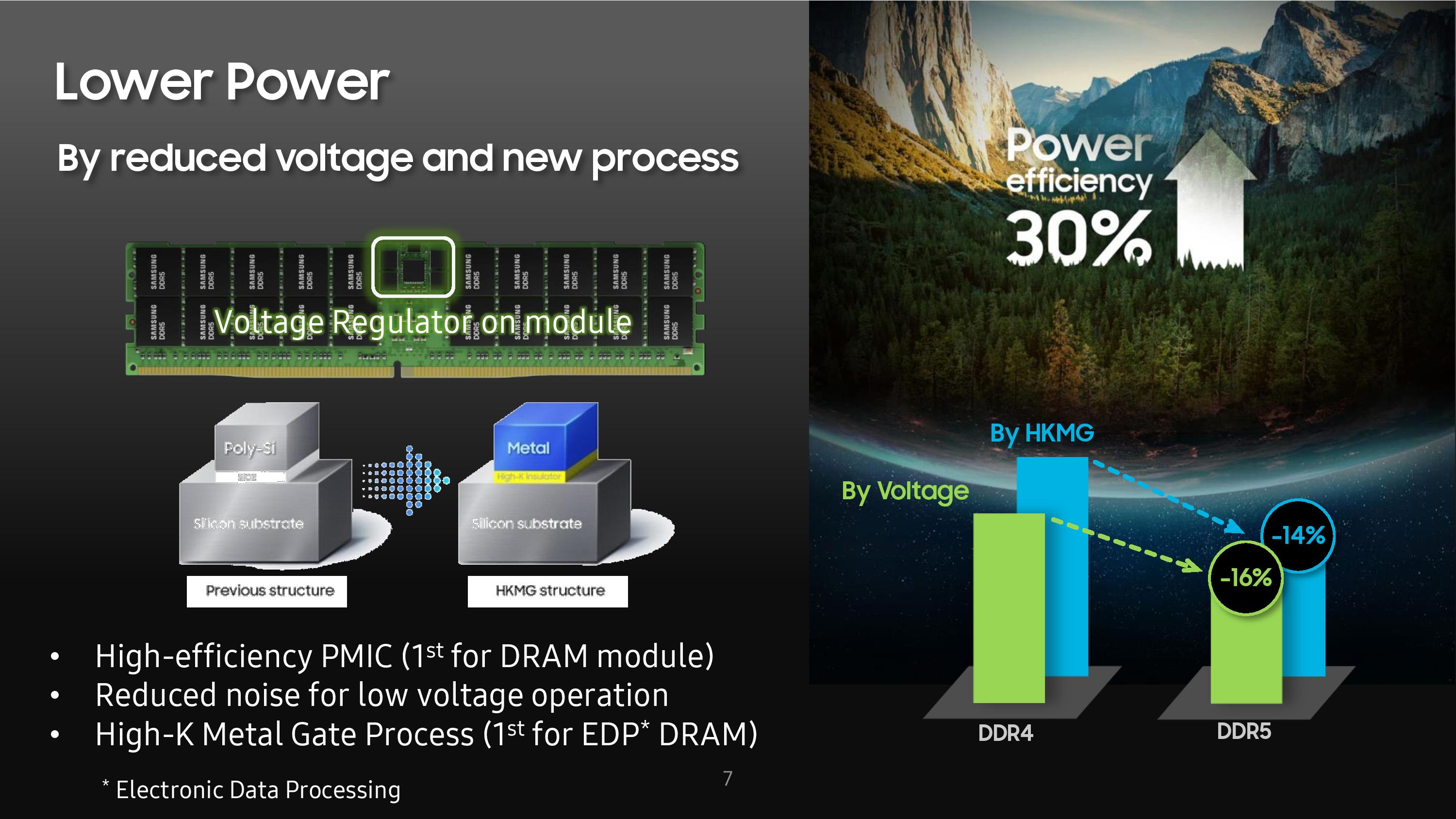
On power, we’ve known that one of the drivers for JEDEC’s newest memory specifications is lower power, and for DDR5 the major thing aside from the lower voltage is to bring the voltage regulator from the motherboard on to the memory module. This allows for the memory module manufacturer to more tightly control the power requirements and consumption of the memory, especially should the motherboard be a very cheap model that might skimp on valued components at the voltage regulation level. For this 512 GB module, Samsung is using a high-efficiency Power Management IC (PMIC) – Samsung as a company has a lot of PMIC experience through its other electronic divisions, so no doubt they can get high efficiency here. Samsung also states that its PMIC has reduced noise, allowing for lower voltage operation, and also uses a High-K Metal Gate process (introduced on CPUs at 45nm) in a first for DRAM.
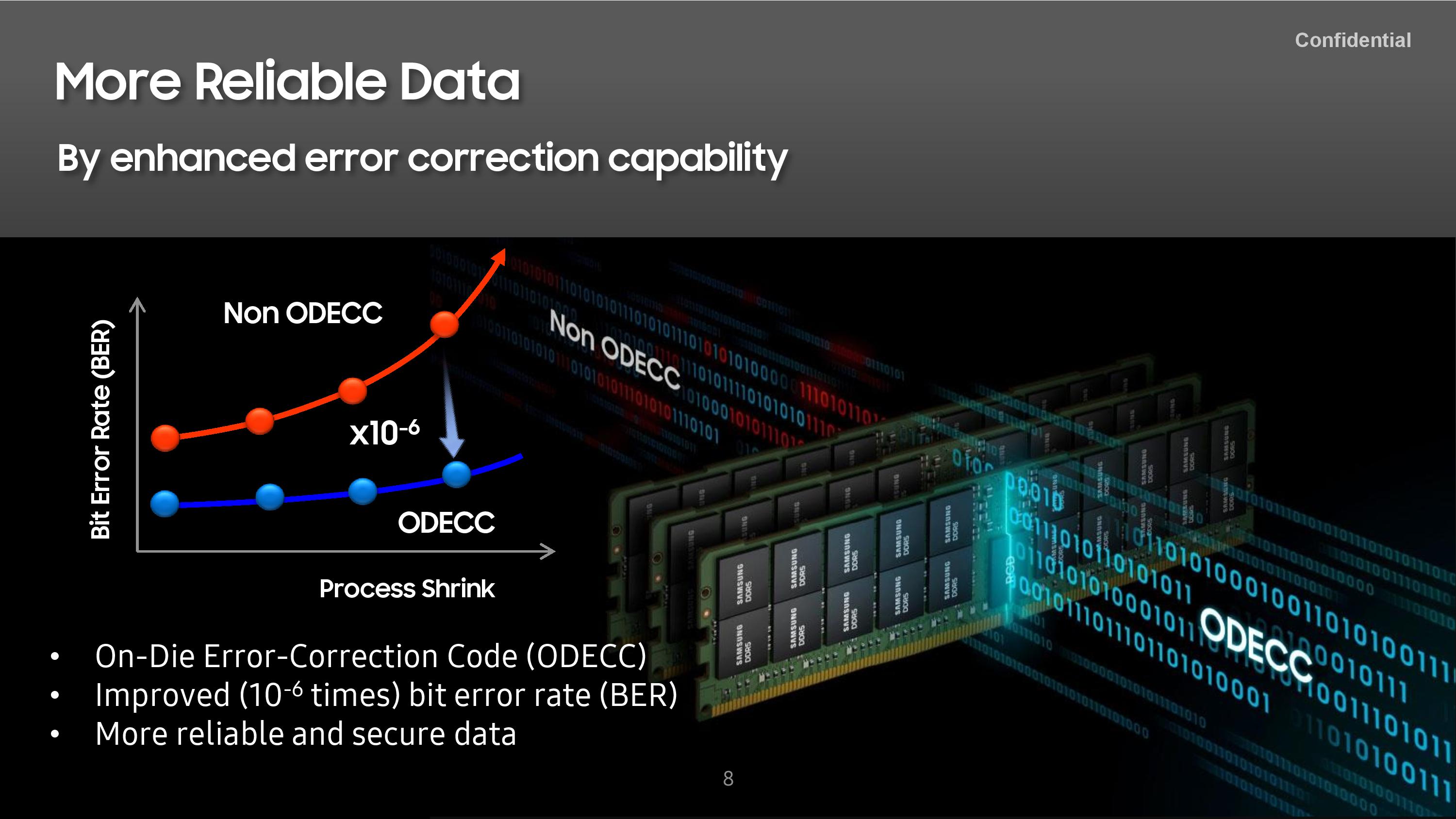
One of the talking points on DDR5 has been the on-die ECC (ODECC) functionality, built in to DDR5 to help improve yields of memory by initiating a per-die ECC topology. The confusion lies in that this is not a true ECC enablement on a DDR5 module, which still requires extra physical memory and a protected bus. But on the topic of ODECC, Samsung is showcasing an improvement on its bit-error rate of 10-6, or a factor of a million lower BER. How much of this is required by the DDR5 JEDEC specification is unclear at this point, but it’s still a good direction to have.
At the end of the slide deck from Samsung, it states that its first 512 GB module should be ready for mass production by the end of 2021 – it’s unclear if this is a DDR5-7200 module or something else, as the slide could be interpreted differently. But one of the key aspects to this discussion is when the market expects the crossover of DDR4 and DDR5 to occur: Samsung has a big window of 2023-2024 planned for that crossover, which does align with other market analyst predictions.
This stuff is still going to cost some serious money, which makes me wonder what this means for consumers. Right now the supply of 32 GB modules (UDIMMs) seems to be plentiful for those that want 128 GB of memory in a consumer system. The advent of these new memory packages from Samsung might suggest a path to 64 GB modules for DDR5 on the consumer platform, however you can bet your bottom dollar that they’ll stay for enterprise for a while as they will command a price premium.
Stay tuned for AnandTech’s Hot Chips content throughout this week.


27 Comments
View All Comments
Kamen Rider Blade - Sunday, August 22, 2021 - link
For this 512 GiB Memory Module:Assuming Double Sided Memory Module with a total of 32 Memory Packages (Not Counting the extra ECC Packages for Parity on each row in each halve of the Memory module)
1 Memory Package = 16 GiB per Package / 8 Layers per Package = 2 GiB per RAM Die Layer
Does my math sound about right?
Kamen Rider Blade - Sunday, August 22, 2021 - link
Do you think Enterprise Customers would ever want to go with Double Height Memory Modules for more RAM?https://www.anandtech.com/show/13694/double-height...
Given the height of the PCB, I can see future DDR5 Memory Modules with more than 2x rows.
Potentially 3/4/5 rows of Memory Packages on each side of the Memory Modules, doubling them for obviously alot more memory.
1 Double-Sided Rows = _256 GiB
2 Double-Sided Rows = _512 GiB
3 Double-Sided Rows = _756 GiB
4 Double-Sided Rows = 1024 GiB
5 Double-Sided Rows = 1280 GiB
Imagine one "Double-Height" Memory Module in a Enterprise Server Rack that contains 1280 GiB or 1.25 TiB of RAM in one Memory Module
Wrs - Sunday, August 22, 2021 - link
Bandwidth is a primary issue such that they’ll be forced to remain wide instead of tall. At some point all that extra RAM is for concurrent tasks on a many-core CPU, not a single user operating on an enormous data set.Kamen Rider Blade - Sunday, August 22, 2021 - link
True, but wouldn't a Double-Height RAM module using DDR5 help facilitate that?More RAM on one PCB. Given that there is a finite amount of DIMM slots on any MoBo, wouldn't more RAM be better?
Wrs - Sunday, August 22, 2021 - link
The primary factor that limits both capacity and bandwidth is the memory controller - usually on the CPU these days - both the width (number of channels) and the technologies employed (DDR generation, buffering). Most workstation/desktop boards already have 2 DIMMs per channel, some servers have up to 6 DIMMs a channel - most uesrs don't hit the maximum DIMM capacity per channel. This means commodity DIMM sticks don't really need to get taller, only the motherboard & CPU need to be designed to accept more sticks.schujj07 - Monday, August 23, 2021 - link
Ice Lake Xeon and Epyc have are 8 DIMMs/Channel.Another issue actually is Z height. 1U servers are 44mm tall and a standard RAM module is 30mm tall. This would mean that a module like this is only useful for 2U or taller servers. That means you won't be able to use it is blades, 2U4Ns, etc... which is popular for compute nodes.
Freeb!rd - Thursday, April 7, 2022 - link
The "Milan" I/O die integrates eight DDR4 memory controllers ( UMC s), two per I/O die quadrant, which achieve data rates from 1333 to 3200 MT/s. Up to 2 DIMMs per channel are supported.May 31, 2021Kamen Rider Blade - Monday, August 23, 2021 - link
Now if Intel & AMD can go OMI for their memory Interface, they can join IBM in revolutionizing the Memory Connection by going for a Serial connection. Get JEDEC to help standardize that sucker, because having RAM still be a direct parallel connection seems like a outdated concept in 2021.By going OMI, you'd get more Memory Bandwidth to the CPU thanks to the OMI and Serial Nature of it's connection with the Memory Controller being simplified and somewhat local to the Memory Module itself with a simple OMI receiver link on the CPU end.
coburn_c - Sunday, August 22, 2021 - link
CL50 huh. So we double the clock speed from 3600 to 7200, then we sit 'round doing nothing for 50 cycles to deal with it. How is this better than the clock at 3600 but only waiting around 16 cycles between operations?lightningz71 - Sunday, August 22, 2021 - link
Larger caches combined with more aggressive prefer hers have been working together for years now to reduce the impact of dram access latency. I suspect that these CL numbers won't be that impactful in practice.