SK Hynix Reveals DDR4-3200 Memory Chips with 4 Phase Clocking
by Anton Shilov on November 16, 2018 2:30 PM EST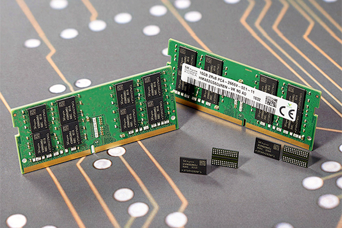
SK Hynix this week announced that it has completed development of its latest-generation DDR4 memory chips. The new DRAM chips are made using the company’s second-generation 10 nm-class fabrication technology (1Ynm) and feature a number of enhancements designed to cut-down die sizes, reduce power consumption, and improve their frequency potential.
At a high level, the new 8 Gb DDR4-3200 chips consume 15% less power than the company's first-generation (1Xnm) DDR4-3200 devices. The process node bump means that their die size has also been reduced by around 20%, which will eventually help to drive down their costs. Initially, SK Hynix will use its 1Ynm technology to make memory chips aimed at servers and client PCs, but eventually the same tech will be applied to LPDDR memory for mobile devices.
In addition to smaller die size and lower power consumption, SK Hynix’s newly developed 8 Gb DDR4-3200 chips feature two important enhancements: a 4-Phase Clocking scheme as well as the Sense Amplifier Control technology. The 4-Phase Clocking increases signal strength to maintain stability at high data transfer rates. Meanwhile, the SAC lowers possibility of data errors that may occur when transistor sizes shrink.
The new DRAM devices from SK Hynix are the first memory chips to incorporate a quad-phase clocking scheme. While SK Hynix conservatively rates the new chips at DDR4-3200, the quad-phase clocking enhancement may potentially enable a higher overclocking potential, though this is something that has to be tested.
SK Hynix has not yet started mass production of DDR4 chips using its second-generation 10 nm-class fabrication technology. Keeping in mind that even the current-gen DDR4-3200 chips are listed as “sampling” at the company’s website, it is likely that the new chips will hit mass production in 2019.
Related Reading:
- SK Hynix Lays Out Plans for 2017: 10nm-Class DRAM, 72-Layer 3D NAND
- Samsung Starts Production of 8 Gb DDR4-3600 ICs Using 2nd Gen 10nm-Class Tech
- Samsung Begins To Produce DDR4 Memory Using '10nm Class' Process Tech
- Samsung & SK Hynix Graphics Memory Prices Increase Over 30% In August
- SK Hynix Announces 8 GB LPDDR4X-4266 DRAM Packages
Source: SK Hynix


4 Comments
View All Comments
.vodka - Friday, November 16, 2018 - link
Maybe these could be worthy contenders to Samsung's B-die DDR4 in high end sticks capable of tight timings + high speeds, unlike the rest of Hynix's current chips.Always_winter - Sunday, November 18, 2018 - link
sounds more like ddr5 will be here before these will or intel 10nm chips and chipsets with 1st gensKevin G - Sunday, November 18, 2018 - link
While DDR5 is starting to sample, no mass production SoC is on the horizon to leverage it in the short term.On the Intel side, it appears that the Ice Lake platform will remain DDR4 for main stream users in 2019 with the 2020 followup using the same platform. The server side will remain with LGA 3467 through Ice Lake-SP which looks to be a 2020 part as well.
AMD has committed to their existing socket platforms through 2020. Thus existing platforms can enjoy Zen 3. AMD's new chiplet strategy does break off the memory controller from the CPU platform (I'm predicting that Zen3 will use the same IO hub as Rome in servers). This would let AMD transition sockets relatively quickly as the CPU side of things is already done. Still I would not expect a new socket from them until 2020 at the earliest.
IBM has a change of leveraging DDR5 first mainly because they are still proprietary fully buffered memory on the high end. One of the advantages here is that the memory type is abstracted behind the buffer thus permitting mixing of memory technologies in a single system. (The older JEDEC FB-DIMM spec even permitted this but I am unaware of any DDR3 based FB-DIMMs ever shipping). IBM has released some research papers exploring even more generic fully buffered memory bus technology, including toying with a full SRAM array in their labs.
sing_electric - Monday, November 19, 2018 - link
To add on to your point re: AMD's Zen architecture and DDR longevity: Without knowing the exact way that Rome works, it seems very likely that AMD will make multiple IO hubs. My bet is consumer-facing parts will have a "cut down" version of the IO hub.Down the road, though, it likely means that AMD will be able to mix/match chiplets, graphics (for APUs) and IO. This means that they could potentially use one chiplet design (Zen 4?) and give higher-end chips (servers, HEDT) DDR5 while using the same/a very similar chiplet and a different IO hub and keep things on DDR4. I wouldn't be surprised if AM4 was kept alive for a very long time, but increasingly relegated to lower-end machines (we might have a time when mainstream Ryzen processors are on a new platform featuring a new socket, DDR5, PCIe 4, while say, their APUs stay with AM4 with DDR4 and PCIe 3).