ChipRebel Releases Kirin 980 Die Shot: Cortex A76's & Mali G76 in View
by Andrei Frumusanu on November 7, 2018 4:30 AM EST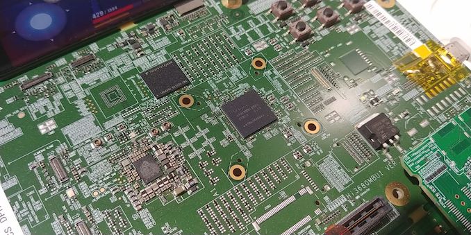
When new flagship silicon chips are released, one thing that I always eagerly await is somebody publishing a die shot of said design. Over the past few years this has always been done by ChipWorks and subsequently TechInsights – but last year a little known site called ChipRebel caught my attention when they released a very high quality, high-resolution shot of the Apple A11. I’ve been in touch with the folks over there over the past few weeks, poking to see what their plans were, and was happy to hear that they’re trying to gain more traction in the future.
Yesterday ChipRebel released a preliminary teardown of the new Huawei Mate 20 – and along with it publicly released a low-res version of their Kirin 980 die shot, along with their commercial high-resolution shot. This is very exciting, as the new HiSilicon chip marks the second commercially available consumer 7nm chip – of course after Apple’s own A12 from just a few weeks prior. More importantly, this is the first time we’re seeing Arm’s new Cortex A76 CPUs as well as the new Mali G76 GPU.
I took the liberty to label some of the some more obvious block complexes of the SoC image on my own, and also shared this with the folks over at ChipRebel:
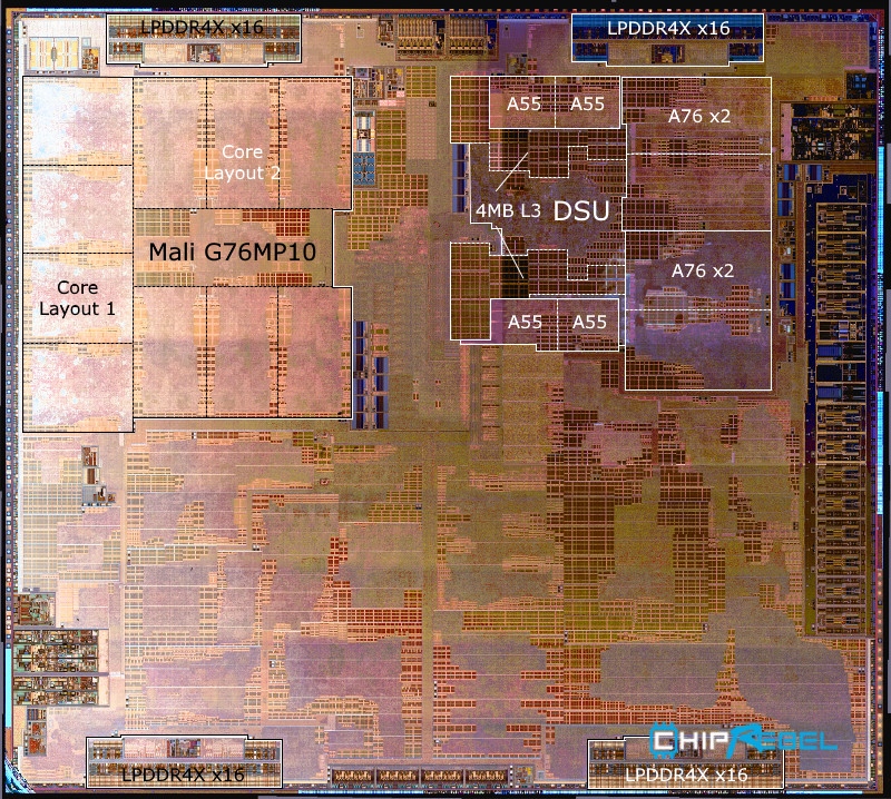
Die shot credit: ChipRebel - Block labelling: AnandTech
Second commercial 7nm SoC - Another tiny die!
First of all – the Kirin 980 is quite a lot smaller than HiSilicon had led to people to believe: Back when the chipset was announced, they had mentioned it was “under 100mm²”, with many thinking the die would be somewhere in the ballpark just below that figure. In reality, the Kirin 980 measures just a mere 74.13mm² - a 30% reduction compared to last year’s 96.72mm² Kirin 970 – even though the new chipset brings a lot of new features and more complexity.
On the top left corner we can see the new Mali G76MP10 GPU. The Mali G76 drastically differs from past generation Arm GPUs in that it essentially doubles the computational capabilities of each core – in effect that one could say that the new MP10 core configuration in the Kirin 980 is about equivalent to a MP20 of the previous generation – microarchitectural improvements aside.
On the right side we see the new CPU complex. This is HiSilicon’s first DynamIQ CPU configuration, as the company’s release schedule for the Kirin 970 last year made them miss out on the Cortex A75. For the Kirin 980 however, we see a configuration that fully takes advantage of the new DynamIQ flexibility: We have essentially one large CPU cluster, with different CPUs attached to it.
The centre complex is the DSU, the DynamIQ Shared Unit, essentially the L3 cache controller along with the tag RAMs as well as the large 4MB L3 cache itself. Flanked on both sides of the DSU we see the 4 Cortex A55 cores that clock up to 1.8GHz, each of these also sport private 128KB L2 caches.
Really nice to see on the die shot is the two pairs of Cortex A76 cores. HiSilicon employs the four cores into pairs, with each pair running on a dedicated voltage and frequency plane. We can see that the physical implementation between the two pairs very evidently differs, and this would confirm my suspicion that we’re looking at a frequency optimised pair, running at up to 2.6GHz, and a more power optimised pair, limited to 1.92GHz. Both pairs employ 512KB private L2 caches on each core.
An interesting thing is that it’s again extremely difficult to even locate the NPU on even the Kirin 980. HiSilicon describes this as a dual-core unit, however I can’t seem to find any matching block on the shot – if the company is using non-identical layouts for the two “cores”, then all bets are off in trying to identify this easily.
Overall, it’s great to have a new player in the die shot imaging scene, and hopefully the folks over at ChipRebel are able to gain more attention in order to be able to continue to share with us images of important future chip developments.
I’m finishing up my review of the Mate 20 and Mate 20 Pro – and we’ll go into more detail into the performance and power of the new Kirin 980 and the new Cortex A76 CPUs as well as the new Mali G76, so stay tuned!


27 Comments
View All Comments
psychobriggsy - Wednesday, November 7, 2018 - link
That improves the transistor density measurement somewhat to 93M/mm^2 - very dense for a real-world design.Valantar - Wednesday, November 7, 2018 - link
I'm always fascinated by just how great a portion of the die is taken up by uncore components. The CPU and GPU clusters here look like they take up ... 30% of the non-I/O parts of the design? A bit more? I guess various interconnects take up a good deal of space, as well as the NPU (even if it can't be easily identified). But the rest? How much space does a video encode/decode block need, even supporting all kinds of codecs at 4k60? And what are those giant caches (I think?) spread across the die for? If the L3 blocks outlined are 4MB, there's at least as much in the blotchy lumps directly below the CPU cluster.It would be incredibly cool if some SoC vendor gave an in-depth explanation of the layout of one of their chips, even an older one like the SD820 or similar, detailing all the various parts and how they are arranged and connected.
Andrei Frumusanu - Wednesday, November 7, 2018 - link
Top off my head:- CPU complexes
- GPU
- NPU
- Modem
- ISP (multiple blocks, multiple cameras)
- DSP
- Video enc & dec
- Image scalers and encoders/decoders
- Sensor hub/microcontroller
- Display controller
- UFS/eMMC controllers
- Peripherals (USB, HSIC, etc)
- A ton of random microcontrollers
- Audio subsystem (CPU and all)
- Secure subsystem (CPU and all)
- Memory controllers
- Interconnects for it all
You can't really hope to identify most of these, especially if they're smaller blocks.
nullington - Wednesday, November 7, 2018 - link
Whats that in the center of the upper edge? NPU?DanNeely - Wednesday, November 7, 2018 - link
stuff on the edge is almost always IO of some sort.nullington - Wednesday, November 7, 2018 - link
It already has the GPU core Layout 1 near the edge.name99 - Wednesday, November 7, 2018 - link
Those are 16 ethernet ports. Did you not know that this thing is also a kick-ass switch?:-)
eastcoast_pete - Wednesday, November 7, 2018 - link
@Andrei: Thanks! Always enjoy your reviews of SoC architecture.Two wishes/requests: 1. Please do a deep(er) dive into the current state of NPUs on current and upcoming mobile SoCs. I was really struck by the size of the NPUs on Apple's A12, but don't know how heterogeneous both architecture/real estate and capabilities (known or rumored) of NPU circuitry are that are found in the A12, the Kirin 980 and the Snapdragon 845. Don't know if Samsung's newest mongoose has any NPUs on it, but I've been wrong before.
2. You'll probably address this as part of your Mate 20/Mate 20 Pro review, but this Kirin may, right now, have the most powerful big core in the mobile space outside Apple's Vortex (big A12 core). Look forward to a side-by-side comparison, as much as this is even possible. Thanks!
Andrei Frumusanu - Wednesday, November 7, 2018 - link
Both will be in the review.skavi - Wednesday, November 7, 2018 - link
Based on this die shot and the A12's, the Vortex and A76 appear fairly similar in size. Are they annotated differently, or are they actually that close?