Hot Chips 2018: Samsung’s Exynos-M3 CPU Architecture Deep Dive
by Andrei Frumusanu on August 20, 2018 1:00 PM EST
As part of this year’s first conference talks at HotChips 2018 at the Flint Center for the Performing Arts in Cupertino, California, we’ve had the pleasure to finally hear Samsung’s official microarchitecture disclosure on this year’s most polarising new CPU design, the Exynos M3.
Our first exclusive report on the details of the new microarchitecture back in January. It was clear at this point from that point on that the design was a big one: Samsung had gone for a huge push in terms of performance, resulting in one of the biggest generational jumps of any silicon CPU designer in recent history.
Over the coming months much of the hype for the new Exynos 9810 with its M3 cores fizzled out, with each bit of additional testing revealing less and less enticing results. Starting from some questionable early-on benchmarks at the release of the Galaxy S9 through to our extremely in-depth Galaxy S9 device and SoC review, later on moving to DIY improvements in attempting to resolve some of the lower-hanging fruit in terms of software issues which hampered the real-world performance of the Exynos Galaxy S9. Throughout these pieces, of course, we had little in the way of official information from Samsung – until today we still didn’t know much about how the M3 microarchitecture actually worked.
Rewinding back two years, we briefly covered Samsung’s initial microarchitecture disclosure of the Exynos M1 at HotChips 2016, which was a great thing to see. While I always prefer to stay on-topic in articles, we’ve never really taken the opportunity to talk that much about Samsung’s design teams – understanding the teams that create these products also gives us a great deal of insight into the products. This has been especially evident over the last few years, with us understanding more about the workings inside of Arm’s Cambridge, Sophia Antipolis and Austin Cortex-A CPU design centres.
Samsung’s CPU IP is developed in Austin, Texas, at “Samsung’s Austin R&D Center”, or SARC. The centre was founded in 2010 with the goal of establishing in-house IP for Samsung’s S.LSI division and Exynos chipsets. Staffed with ex-AMD, ex-Intel and various other talented industry veterans, what we saw come out - alongside memory controllers and custom interconnects - was also the of course more visible IPs: Samsung’s first custom CPUs.
The Exynos M1 is said to have started its design cycle sometime in 2012 and saw a quite short 3 year development phase, starting from scratch to first tape-out. It made its first appearance in the Exynos 8890 in the 2016 Galaxy S7. Over the years SARC has been expanding, and in 2017 the Advanced Computing Lab (ACL) in San Jose was opened and added to the SARC’s joint charter – adding custom GPU IP to its design portfolio that we hope to see productised in a couple of years.
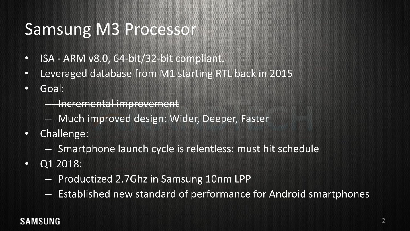
The Exynos M1 being designed from scratch, it’s natural to expect that follow-up generations would be using it as the starting point for further development. Following the tape-out of the M1, the SARC team started off the M3 design with the existing M1 RTL back in Q1 of 2015. At first, this was meant to be an incremental development. However, there was a larger change of plans later on in Q1 2016, as goals were set higher for a much larger performance push.
The existing improvements were forked in Q3 2015 into what became the M2 – which was initially meant to only be a 10LPE port of the M1 (Which was 14LPP). As a reminder, the M2 had a robust ~20% IPC improvement across workloads, which allowed it to outperform the M1 even though it was clocked 12% slower in production silicon. Samsung had achieved this by implementing some of the originally planned M3 features into the M2, while the new M3 design became more aggressive.
Here Samsung clearly states one of the industry’s most unforgiving aspects: a relentless launch cycle in which the IP and silicon must be in sync with. Many issues that we’ve seen in SoCs from various vendors, both in terms of performance and especially in terms of power consumption are mostly due to the fact that there was a rush to market in order to catch the commercial release window for new products.
Samsung's Exynos M3 - Introducing Meerkat
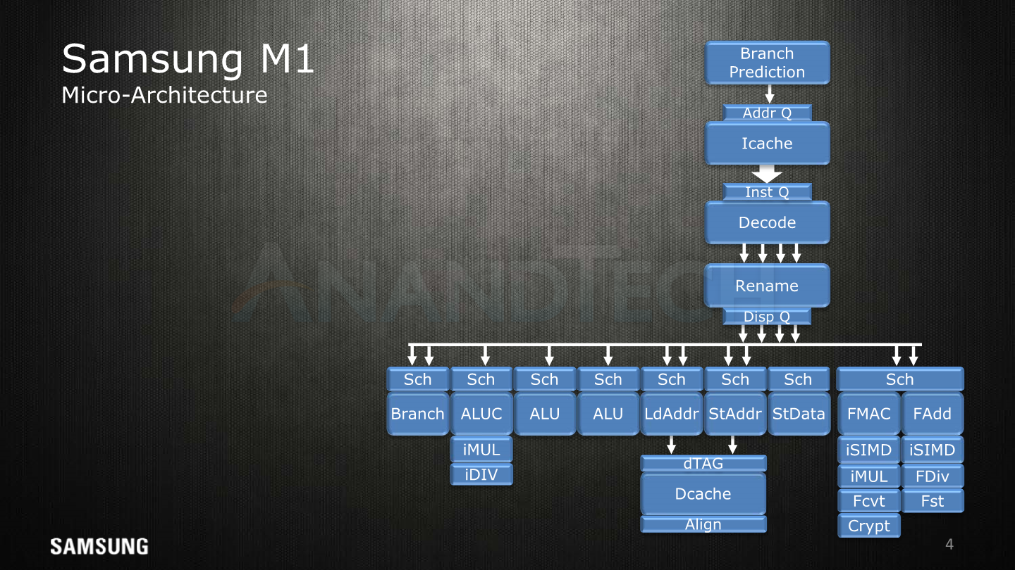
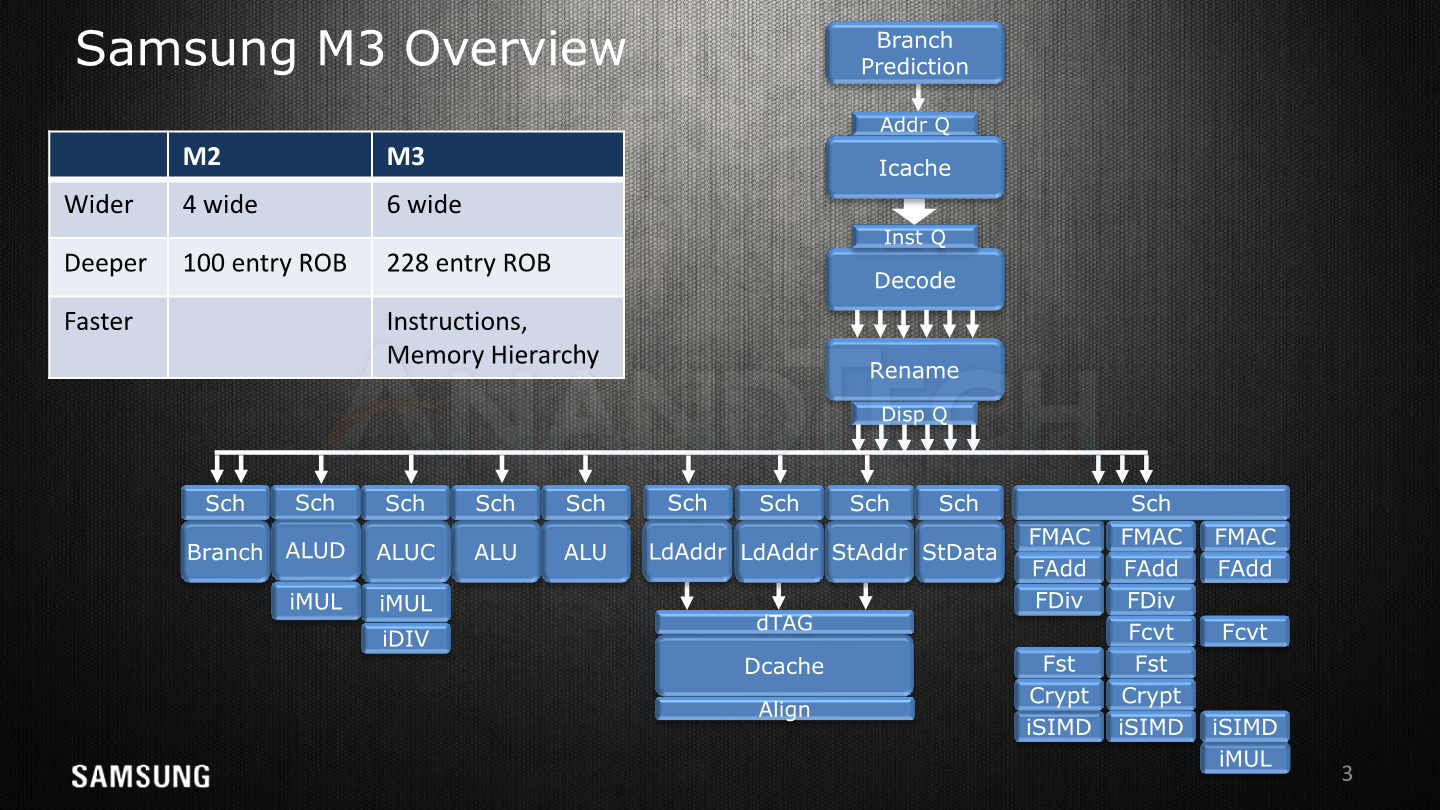
Starting off with a high-level overview of the Exynos M3 alongside with the original slide of the M1, we see big similarities, yet the M3 just adds more onto the table. The SARC team increased the microarchitecture width from a 4-wide decode unit to a 6-wide, the overall core defining characteristic of the new µarch. We see an added integer ALU with multiplier capability, a second load unit and a vastly expanded floating point / SIMD complex with up to triple the compute capacity.
We never really had a microarchitecture disclosure of the M2 and there’s also no specific compiler machine model tied to it, but among one of the changes revealed today is that the reorder buffer has seen a minor adjustment from 96 to 100 entries. As mentioned in our first µarch disclosure back in January, the M3 vastly expands this to up to 228 entries, making this aspect of the µarch a lot more similar to the what we see in Intel’s core designs - although we can’t make a direct density comparison across different ISAs as instruction complexity varies.
When Arm disclosed the A76 µarch details and particularly the 128-entry ROB (which in comparison seems quite small to the M3), they said that this was a balance between performance and area/power. In particular we saw a mention that a 7% increase in the ROB capacity only came with a 1% performance gain on average.
Samsung explains that ROB capacity is a choice which is tied to the design of the rest of the microarchitecture and the various buffers and backend scheduler capacities – µarch depth and µarch width are complementary to each other for performance. A wider µarch such as the M3 is able to fill the ROB faster and thus get more performance return out of the larger capacity. Overall the M3 is said to have been made with a different set of decisions than the M1/M2, aiming for the higher performance while taking into account the associated costs.
A Much Larger Front-End
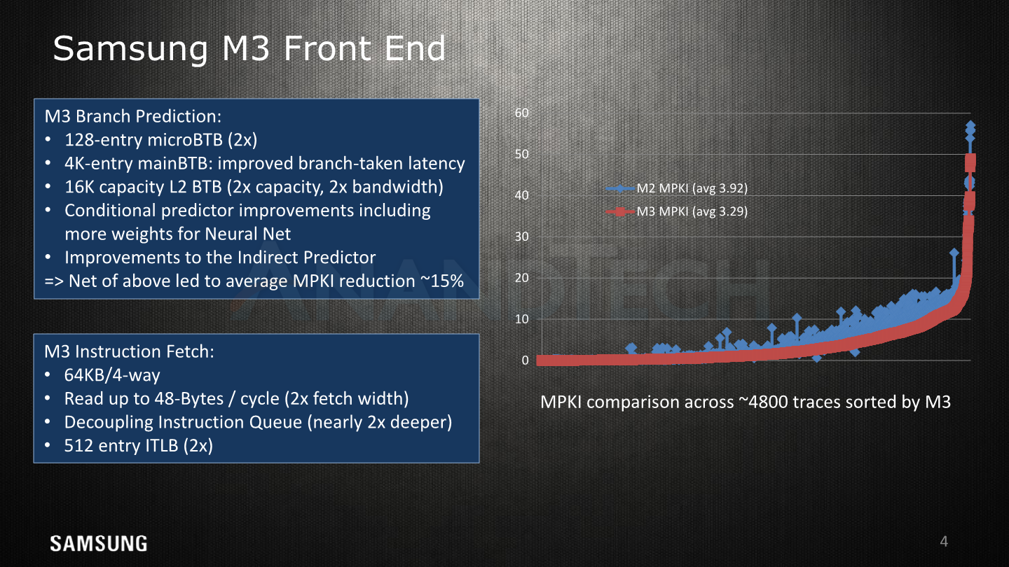
Diving into more details on the front-end, we see the various improvements on the branch predictor and fetch units. The M1’s branch predictor differed from other µarch’s in that it was able to take two branches per cycle and having two branch ports on the backend. The M3 seems to maintain this width, but doubles up the µBTB from 64 to 128 entries. The mainBTB remains at 4K entries but has had latencies improved for taken branches.
On top of this the branch predictor quality overall has been increased – resulting in a 15% average reduction in missed branches. It was interesting to see Samsung actually publish an actual MPKI (Misses per kilo instructions) value here as it's something we haven’t seen acknowledged by Arm (or any vendor?) to date. Here Samsung monitors a continuously expanding suite of 4000-6000 code traces from various applications and use-cases against which it validates its performance against during development.
The branch predictor and fetch units respectively feed a decoupled address queue and a decoupled instruction queue, this is likely done so that the units can be clock gated in the implementation.
The fetch unit’s bandwidth has been doubled and now can read up to 48 bytes per cycle which corresponds to 12 32b instructions per cycle – this results in a 2:1 ratio of fetch versus decode capacity which is an increase over the 1.5:1 ratio (24B/c, 4 decode) in the M1. Samsung explains that the big increase is needed to combat the increasingly big problem of branch bubbles on wider microarchitectures. They admit that on average, the distance between taken branches is less than 12 instructions, but the larger width helps a lot for temporary bursts of instructions.
While this change has a high instantaneous power utilisation, when the instruction queue (which is now double the depth) gets filled faster than the decode unit can drain it, it has an overall net positive effect on power used as it allows the fetch unit to be clock gated. Here the overall energy efficiency is more tied to the branch predictor quality as it doesn’t actually matter when an instruction is fetched, only with a larger “batch” such as implemented here, there might be more overhead in the thrown away instructions in case of a wrongly taken branch path.
The instruction cache / L1I comes at 64KB. We’re not sure if this is an increase over the M2 as it’s hard to measure, but it definitely is double the size of the M1 µarch.
The instruction translation lookaside buffer (ITLB) has grown from 256 to 512 entries. It’s to be noted here that Samsung is employing a three-level hierarchy as opposed to what we see in Arm’s processors. The A75 and A76 respectively have a first-level 32 and 48-entry µITLB, with a clustered mainTLB of a total of 1280 entries, consisting of 1024 entries for pages up to 64KB and a secondary 256-entry table for pages >=1MB.
Samsung has a first level data and instruction TLB as well, but doesn’t disclose the size of the L1 ITLB. The last level unified TLB for Samsung is also larger at 4096 entries, we’ll come back to it on a later slide.


45 Comments
View All Comments
HStewart - Monday, August 20, 2018 - link
One thing I curious is why does Samsung use this CPU in Europe products and use SnapDragon in US, Japan Markets - Only thing I can think of regulations for security on the chips.Great_Scott - Monday, August 20, 2018 - link
My understanding is that the US version uses the SnapDragon for the integral modem.I'm not exactly sure why this is, it might be an artifact of needing legacy CDMA support for Verizon/Sprint, which isn't needed for a world-phone.
beginner99 - Tuesday, August 21, 2018 - link
That is what I thought as well. CDMA. Not needed for rest of the world.abufrejoval - Friday, August 24, 2018 - link
Unless you assume that some people actually travel. You might even argue that the average European is more likely to enter CMDA space in his life-time than the other way around: Most US citizens only ever leave the country to fight a war, I keep hearing.I prefer to chose myself than have choices mandated to me based on where I tend to be most of the time.
Ej24 - Friday, August 24, 2018 - link
Samsungs own Shannon modem works on CDMA. My galaxy S6 on Verizon Wireless is proof of that. It's probably legal reasons, patents, licensing whatever. It's annoying. Because the Qualcomm has put out some duds and we don't have a choice.az060693 - Monday, August 20, 2018 - link
It's supposedly due to a 1993 patent licensing deal- https://www.androidcentral.com/qualcomm-licensing-...Though in certain phone generations, it might have also been to supply issues.
HStewart - Monday, August 20, 2018 - link
That sounds about right - but I believe the Qualcomm version is faster than the Samsung version. This is a problem with have Modem built into chip - you have to used different CPU depending on which modem is in the SOC,bebby - Tuesday, August 21, 2018 - link
There is another more or less official reason - to reduce risks - instead of only relying on one chip, they use 2, one in-house designed and one external, in case the internal chip has issues. Samsung anyhow manufactures both in-house.name99 - Monday, August 20, 2018 - link
At least one reason they use Snapdragon is for markets that still require voice CDMA, which QC modems provide.aryonoco - Monday, August 20, 2018 - link
The S6 showed that Samsung has no problems making integrated CDMA modems.