The Crucial MX500 500GB SSD Review: A Second Look
by Billy Tallis on February 2, 2018 9:30 AM ESTAnandTech Storage Bench - Heavy
Our Heavy storage benchmark is proportionally more write-heavy than The Destroyer, but much shorter overall. The total writes in the Heavy test aren't enough to fill the drive, so performance never drops down to steady state. This test is far more representative of a power user's day to day usage, and is heavily influenced by the drive's peak performance. The Heavy workload test details can be found here. This test is run twice, once on a freshly erased drive and once after filling the drive with sequential writes.
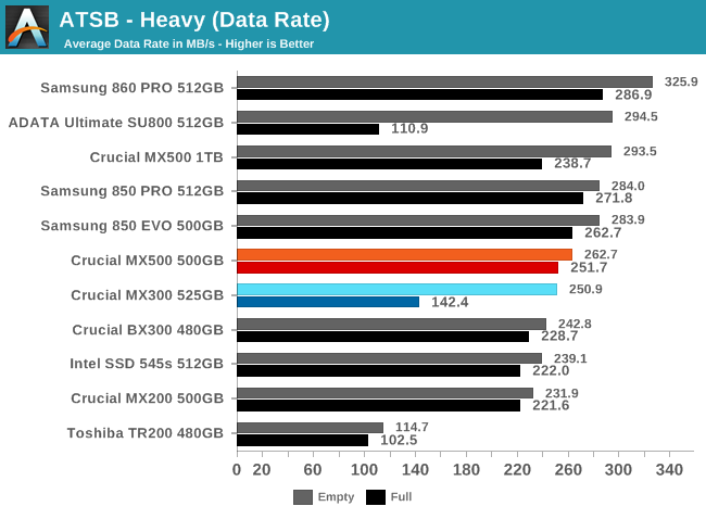
The average data rate of the Crucial MX500 on the Heavy test is barely improved over the MX300 when the test is run on an empty drive, but the full-drive performance is vastly better; the MX500 suffers very little when full. Compared to competing SSDs, the MX500 still isn't the fastest TLC SSD, but this time the Intel 545s is slower while the Samsung 850 EVO is the one that beats the MX500.
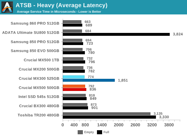
With only a few exceptions, the average and 99th percentile latencies of mainstream SATA SSDs are all in the same general range. The Crucial MX300 was one of the outliers with its poor full drive latency, but the MX500 resolves that problem.
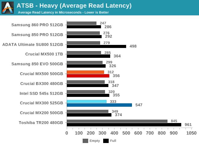
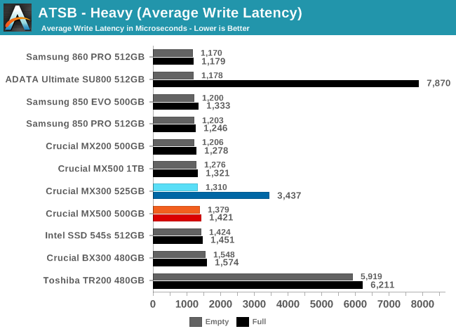
Average read and write latency scores from the Crucial MX500 are reasonable for both the full drive and empty drive test scenarios. The MX500 is still not the fastest TLC drive, but it is never very far behind.
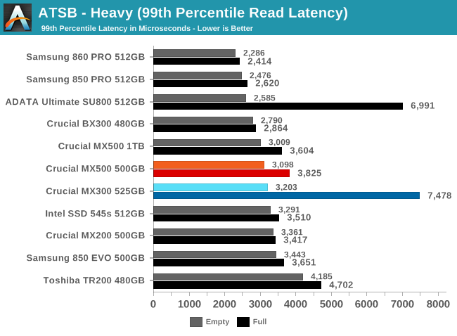
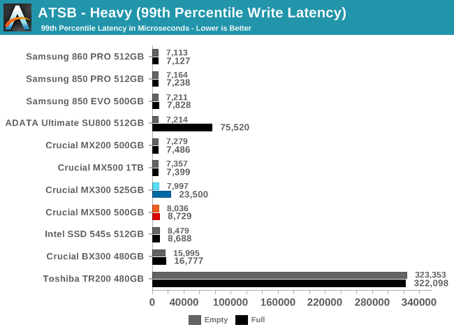
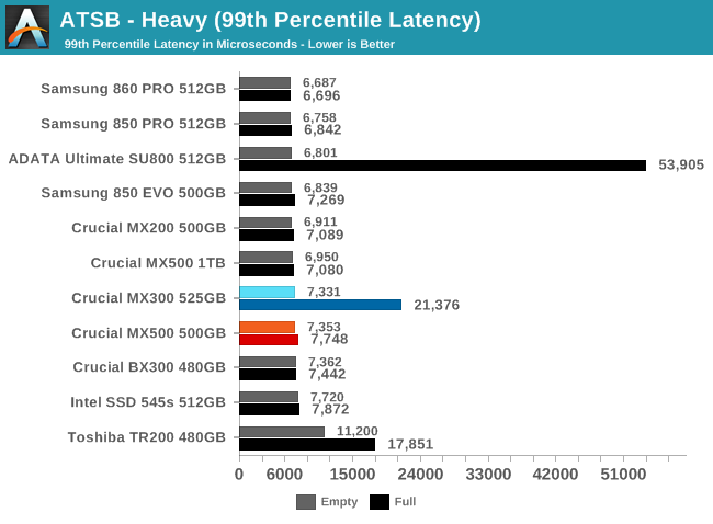
The Crucial MX300 had one of the worst 99th percentile read latency scores when full, but the MX500 has much better quality of service—though still marginally worse than other mainstream SATA SSDs. For 99th percentile write latencies, the MX300's full-drive problems weren't as severe as those suffered by competitors like the ADATA SU800, but the MX500 still straightens things out and ends up scoring better than the MLC-based BX300.
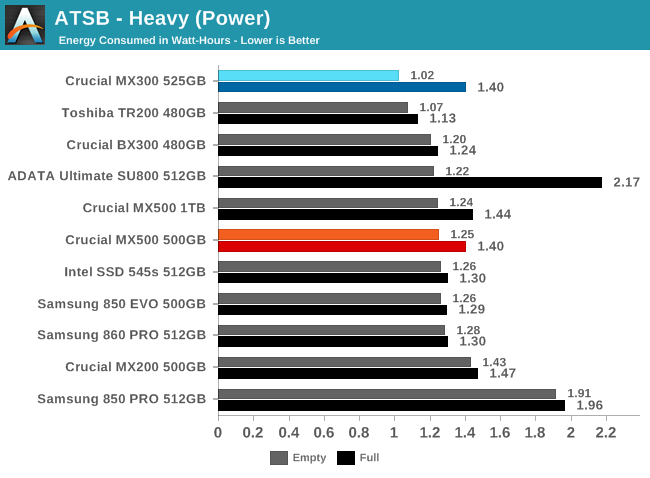
Energy usage for the MX500 over the course of the Heavy test has regressed compared to the MX300, but this only brings the MX500 in line with the rest of the mainstream TLC competition. Full-drive energy consumption is slightly higher than the other recent drives.


25 Comments
View All Comments
PeachNCream - Friday, February 2, 2018 - link
"..the per-die capacity of the MX500's 64-layer 3D TLC is actually lower than that of the 32L 3D TLC.."Why is that the case? Shouldn't doubling the number of layers lead to greater capacity and does this mean that there are more ICs per GB in the newer MX500? I'm super confused.
jtd871 - Friday, February 2, 2018 - link
"The Crucial MX500 uses Micron's 256Gb 64L 3D TLC part and consequently returns to the standard drive capacities and overprovisioning ratios, instead of the unusual configurations caused by the 384Gb die capacity in the MX300's 32L 3D TLC. The slightly lower usable capacities of the MX500 than the MX300 means the new drives have slightly higher prices on a per-GB basis, but the MSRPs are still very competitive against current street prices for the competition."So the new chips have more layers per package, but less overall capacity. I'll guess the 384Gb die hamstrung performance on relatively smaller-capacity drives by offering fewer memory channels for the processor to work with simultaneously. Plus, I'll guess that it was a bit of an oddball size for the algorithms to deal with.
FunBunny2 - Friday, February 2, 2018 - link
large node?more area dedicated to control functions?
Billy Tallis - Friday, February 2, 2018 - link
For the 32L node, IMFT was more or less prioritizing MLC use cases by making a 256Gb MLC die that could be used as a 384Gb TLC part. For the 64L node, TLC is the priority and they're making both 256Gb TLC and 512Gb TLC parts. The latter should be cheaper per GB when it is available, but would be a worse choice for small consumer drives. The 256Gb die is really tiny, which makes it more appealing to the mobile market than a lot of previous IMFT parts.FunBunny2 - Saturday, February 3, 2018 - link
"making a 256Gb MLC die that could be used as a 384Gb TLC part."so... does this mean that NAND is all the same, and it's the controller that decides among S/M/T?? or is it the case that S can be coerced to M, and M to T, but not the other way round? is there a tute, here or elsewhere, that tells us the nittygritty about why titular NAND can/can't be used at other densities?
FunBunny2 - Saturday, February 3, 2018 - link
well, I did find one, but from 2012 (and AT: https://www.anandtech.com/show/5067/understanding-... )"This array can be turned into either SLC, MLC, or TLC. The actual array and transistors are equivalent in all three flash types; there is no physical difference. "
some/many folks have been claiming that TLC, in particular, is physically different from SLC. is that now true?
Kristian Vättö - Sunday, February 4, 2018 - link
In terms of memory cell design, SLC, MLC and TLC can be the same, but the peripheral circuit design isn't (min # of latches = # of bits per cell). More bits per cell designs are also likely to have more spare/ECC bytes per page.In layman terms, TLC and MLC can be run as pseudo-SLC by only programming the lower page, but it's impossible to run e.g. MLC as TLC. But pseudo-SLC isn't the same thing as native SLC.
Spatty - Wednesday, February 14, 2018 - link
SLC/MLC chips are physically the same chips during the fab process. Maybe some Implant changes but die layout is the same. In Probe, circuits are blown to make them SLC or MLC.The referenced quote in this thread, is that a due to the usage of die vs chip/package. The chips in the images can have multiple die in one single chip/package and thus the 'density' of the chip/package changes. More layers still means more bits/mm^2.
PeachNCream - Monday, February 5, 2018 - link
Thanks Billy! It makes more sense now.colonelclaw - Friday, February 2, 2018 - link
I'm wondering, would it be worth adding a PS4 Pro/'BoneX benchmark to SATA SSD reviews? The 1TB is fast becoming a worthwhile, if luxurious, upgrade for the top consoles. It may be slightly unaffordable now, but possibly not for long?