AMD Threadripper 1950X and 1920X Out August 10th, New Eight-Core TR 1900X at $549 due Aug 31st
by Ian Cutress on July 30, 2017 10:30 PM EST
One of AMD’s skills in recent quarters is the ability to drip feed information about upcoming products slowly to the point where even the breath of a clock speed becomes another several column inches about an upcoming platform. Today’s announcements are as juicy as an average minute steak, giving details confirming the launch dates for the first two Threadripper processors, some in-house performance comparisons, and also information about a third cut of the ingot coming at the end of the month.
Related Reading
- The AMD Zen and Ryzen 7 Review: A Deep Dive on 1800X, 1700X and 1700
- The AMD Ryzen 5 1600X vs Core i5 Review: Twelve Threads vs Four at $250
- The AMD Ryzen 3 1300X and Ryzen 3 1200 CPU Review: Zen on a Budget
- AMD Launches Ryzen PRO CPUs: Enhanced Security, Longer Warranty
- How To Get Ryzen Working on Windows 7 x64
- AMD Launches Ryzen: 52% More IPC, Eight Cores for Under $330
Threadripper Gets a Launch Date
The news at the top of the hour is the date at which AMD is making Threadripper and associated TR4 based motherboards available at retail: August 10th. This is expected to be a full worldwide retail launch, so don’t be surprised if your favorite retailer starts posting teaser images about how much stock they have. August 10th will see both the 1950X and 1920X with their retail packaging, along with motherboards from the main four motherboard vendors.
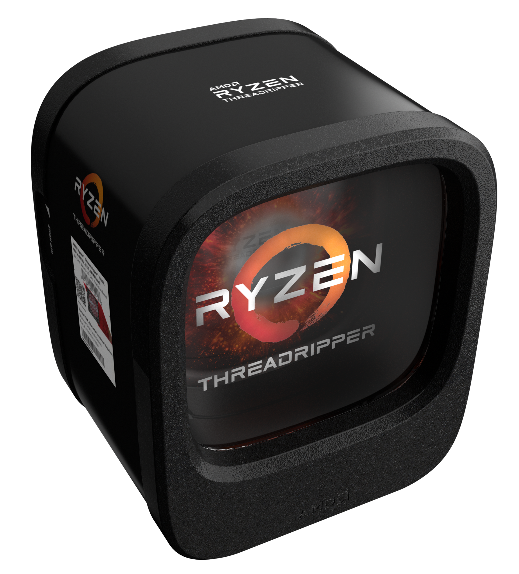
The image used up the top was posted on Twitter a few days ago by AMD showing the retail packaging, and a Dr Lisa Su, CEO of AMD, for scale. The base retail package does not come with a cooler, but does come with a spacer and Torx wrench, as the socket requires a full Torx screwdriver to access it. AMD has engineered an ecosystem of both closed liquid loop coolers partners, as well as a few air coolers capable of meeting the 180W TDP required. We’re looking into exactly which models will have the appropriate support.

AMD is allowing pre-orders for partner systems and boutique OEMs to start from July 31st. Dell’s Area-51 Threadripper edition has been highly covered already, and it was always a question as to why they were allowed to announce earlier than everyone else. The answer was that they secured an exclusive, but it seems only for four days, from the 27th. Nonetheless, other system integrators such as MainGear, OverclockersUK, iBUYPOWER, Origin, Velocity Micro and others will be showing systems from today.

From the motherboard vendor side, this week has seen the main four companies lift the lid on some of their AM4 designs further to what we saw back at Computex. ASRock, ASUS, GIGABYTE and MSI will all be launching motherboards on day one, making full use of the quad channel memory with two DIMMs per channel and 60 PCIe lanes for add-in cards (using another four for the chipset, which we typically do not count to some users’ chagrin). We’re planning a full overview of each board, but keep eyes out for:
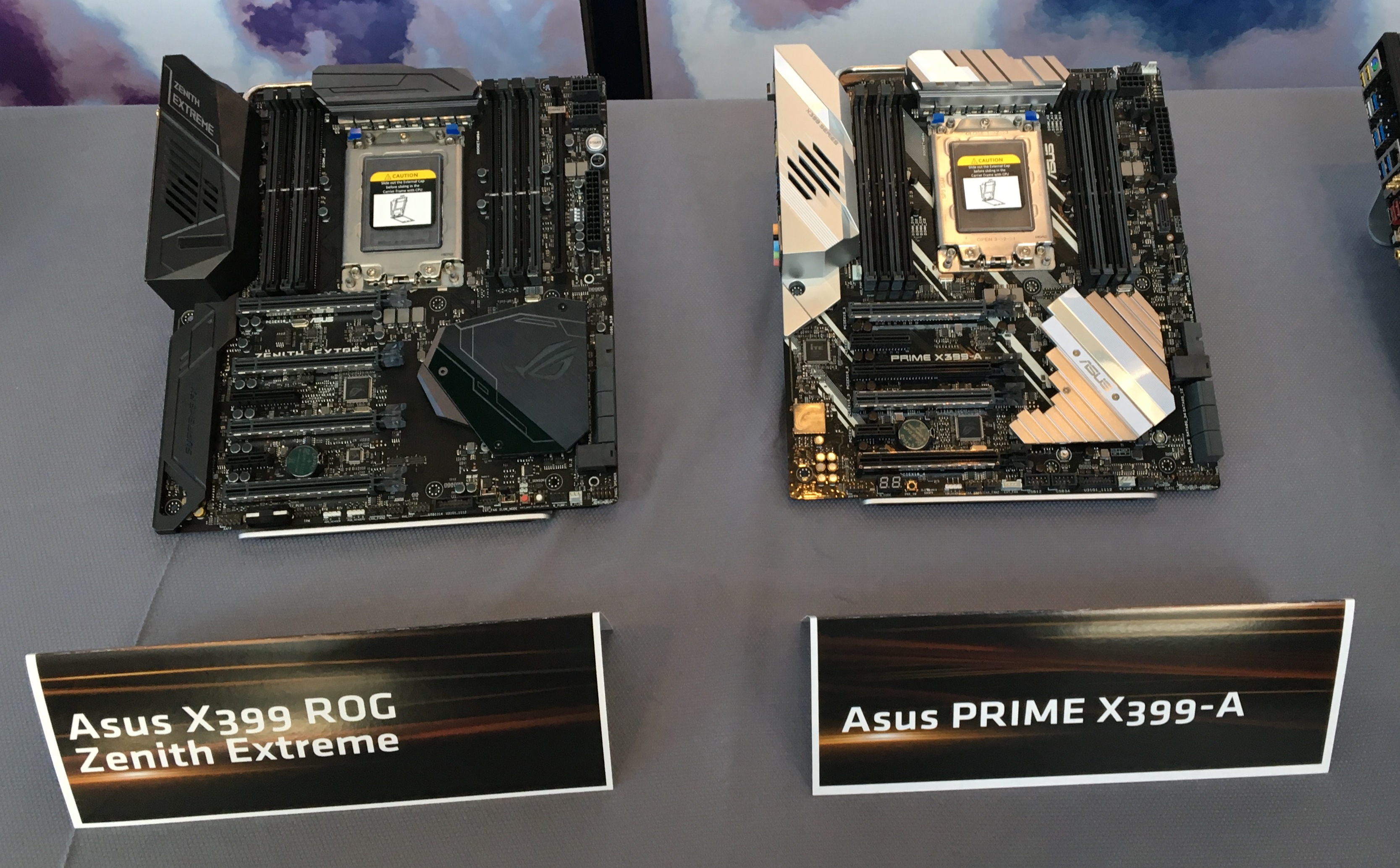 ASUS X399 ROG Zenith Extreme and ASUS PRIME X399-A
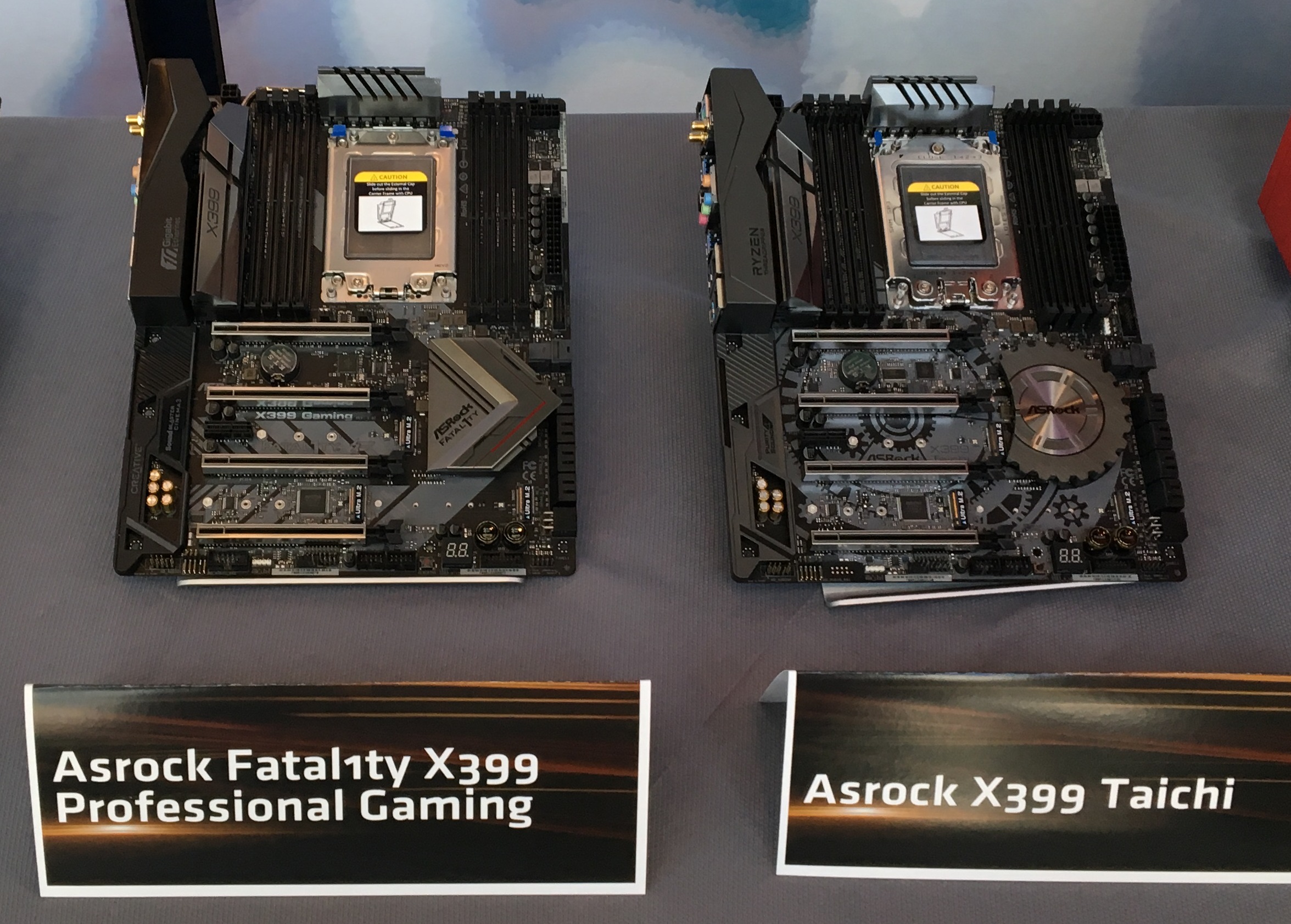
ASRock X399 Professional Gaming and ASRock X399 Taichi
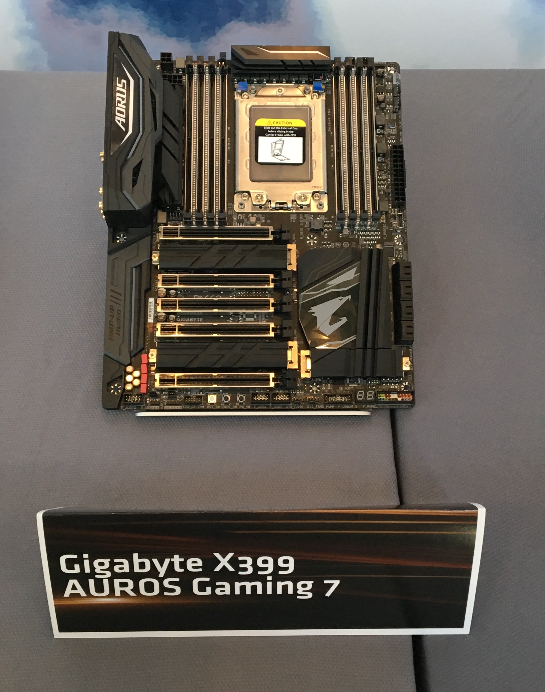
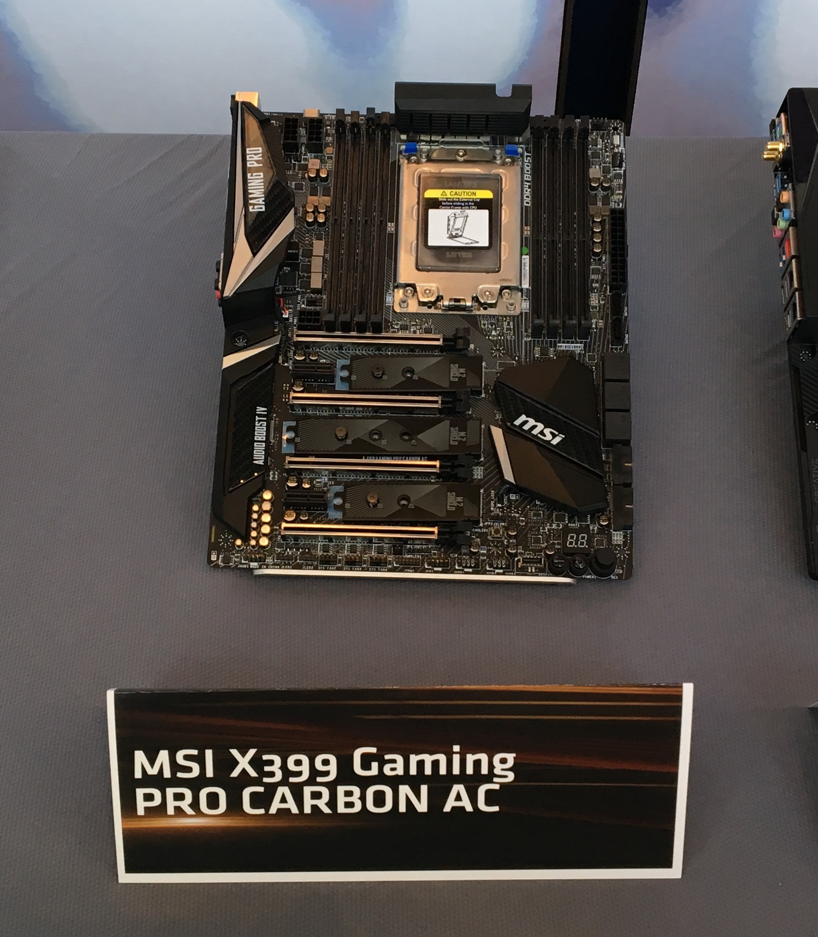
GIGABYTE X399 Gaming 7 and MSI Gaming PRO CARBON AC
At present all the boards being shown are ATX or E-ATX. We’re unlikely to see any mini-ITX due to the size of the socket however microATX might be possible further down the line. No word on pricing for these yet, except that one of the system integrators has priced the ASUS X399 Zenith at +$227 over the GIGABYTE X399 Gaming 7 in their configurator, which suggests the boards will range in price from $300 to $600 pretty easily (add in some knowledge we already have on the BOM cost of some of these parts).
Threadripper 1950X Performance: AMD Gave A Number
Having a few threads in hand at a high frequency means that any benchmark which is thread dense and register light is going to scale very well. AMD shared one data point (which we cannot confirm) from their recent favorite benchmark, Cinebench R15.
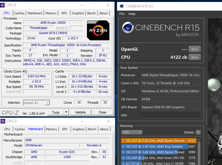
The number given was 4122, representing a 5.2 GHz overclocked (under liquid nitrogen, so not a daily OC) Threadripper 1950X. If we scale this down to 3.5 GHz for the all-core turbo of 1950X, we get a score more around 2774. One of the scores in the screenshot above is 3099, which equates to a 3.9 GHz all-core frequency.
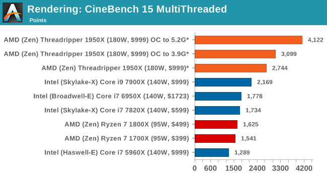
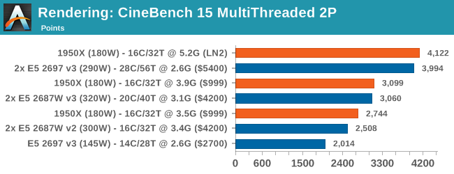
We have some old dual socket CB15 numbers in our database, under Windows 7. There are a fair number of old dual socket workstations around for compute tasks, and TR 1950X (if these numbers are true) beats systems such as a dual socket Ivy Bridge-EP based E5-2687W v3 when running all cores near turbo frequency, which would have retailed at launch for $4200+ just in processors and at a much lower TDP than two of the older processors combined.
Threadripper The Third: The Threadripper 1900X at $549, coming August 31st
To sprinkle some salt onto the steak today is the announcement of a third TR processor. The 1900X is an eight-core part, with a base frequency of 3.8 GHz, a turbo of 4.0 GHz, and +200 MHz of XFR.
| AMD Ryzen SKUs | |||||||||
| Cores/ Threads |
Base/ Turbo |
XFR | L3 | DRAM 1DPC |
PCIe | TDP | Cost | Cooler | |
| TR 1950X | 16/32 | 3.4/4.0 | ? | 32 MB | 4x2666 | 60 | 180W | $999 | - |
| TR 1920X | 12/24 | 3.5/4.0 | ? | 32 MB | 4x2666 | 60 | 180W | $799 | - |
| TR 1900X | 8/16 | 3.8/4.0 | +200 | ? | 4-Ch | 60 | ? | $549 | - |
| Ryzen 7 1800X | 8/16 | 3.6/4.0 | +100 | 16 MB | 2x2666 | 16 | 95 W | $499 | - |
| Ryzen 7 1700X | 8/16 | 3.4/3.8 | +100 | 16 MB | 2x2666 | 16 | 95 W | $399 | - |
| Ryzen 7 1700 | 8/16 | 3.0/3.7 | +50 | 16 MB | 2x2666 | 16 | 65 W | $329 | Spire |
| Ryzen 5 1600X | 6/12 | 3.6/4.0 | +100 | 16 MB | 2x2666 | 16 | 95 W | $249 | - |
| Ryzen 5 1600 | 6/12 | 3.2/3.6 | +100 | 16 MB | 2x2666 | 16 | 65 W | $219 | Spire |
| Ryzen 5 1500X | 4/8 | 3.5/3.7 | +200 | 16 MB | 2x2666 | 16 | 65 W | $189 | Spire |
| Ryzen 5 1400 | 4/8 | 3.2/3.4 | +50 | 8 MB | 2x2666 | 16 | 65 W | $169 | Stealth |
| Ryzen 3 1300X | 4/4 | 3.5/3.7 | +200 | 8 MB | 2x2666 | 16 | 65 W | $129 | Stealth |
| Ryzen 3 1200 | 4/4 | 3.1/3.4 | +50 | 8 MB | 2x2666 | 16 | 65 W | $109 | Stealth |
There are some questions around why AMD would release an 8-core Threadripper, given that the Ryzen 7 1800X is also eight core and currently retails around $399 when distributor sales are factored in. The main thing here is going to be IO, specifically that the user is going to get access to quad channel memory and all the PCIe lanes required for multi-GPU or multi-add-in cards, along with a super high-end motherboard that likely contains multiple CPU-based PCIe x4 storage and/or 10G Ethernet and additional features.


Naturally, with the eight cores being split over two Zeppelin dies (see side note), there is going to be some extra latency between the cores on each of the dies. AMD is countering this by having a higher base frequency (due to the TDP headroom), and stating that the chip allows overclocking. Obviously, some fine-tuned crank is needed and with any luck, it should run 4.0 GHz on all cores.
That Side Note
In the last week, Caseking system builder and overclocker Der8auer (Roman Hartung) released a video de-lidding a supposed Threadripper engineering sample, to which the video was taken down at the request of AMD less than 24 hours later. In the video, he showed that underneath his engineering sample (the ones that AMD gives to system integrators like Caseking to configure systems they will make available) were four silicon dies:
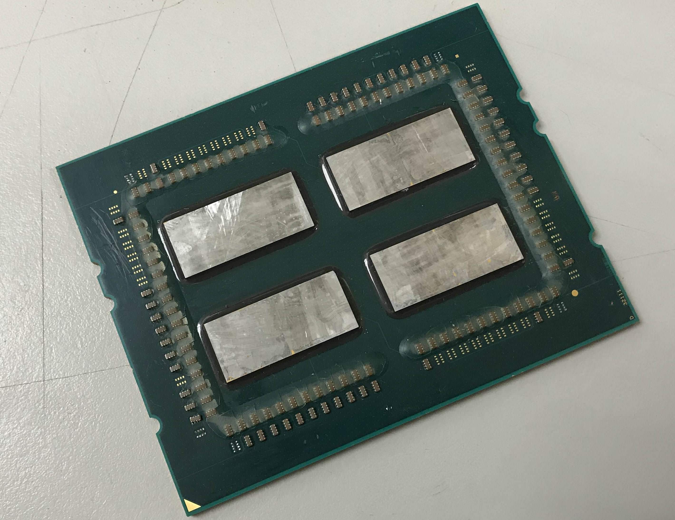
Obviously with Threadripper only going up to 16 cores, and EPYC which uses a similar package going up to 32, we were expecting to see TR with only two bits of silicon, not four. Roman states that only two of the dies are enabled, which simplifies things, but there are a few caveats here to note.
First, this was a Threadripper ES and the retail chips could be quite different. Roman deliberately covered up the markings on the processor on the video (although some images got out), and it was unclear what stage ES this was – as AMD could very likely just give half-disabled EPYCs with different notches in the first ES batches. Simply put, retail Threadripper chips could only have two.
There are several reasons why there could be four though. One suggestion is that these are ‘failed’ EPYCs, although AMD would say that is not the case. If AMD were putting four die onto a chip and disabling two, that would be really bad for the price on return per die, so what is going on here? Simply put, the two ‘disabled’ die aren’t engineered silicon at all, just simple silicon that hasn’t been put through the manufacturing process and added in as spacers for package rigidity. With the Threadripper package being so large, having four places for the mass of the coolers to press onto in the socket for better contact with the socket pins, using spacers would help spread that weight around. There have been suggestions it might help with heat dissipation, but that is unlikely as any heat transfer would be through the TIM and the HS, not through the package itself which is fairly thermally insulating.
To sum up:
- This is an early Engineering Sample, and might not be indicative of retail
- Only 2 of the 4 dies are even active
- If it is retail, 2 inactive dies are likely empty silicon for rigidity
If this is even indicative of a Threadripper retail sample (again, no confirmation it is), our guess is that these two extra ‘dies’ is just empty silicon used for rigidity. So anyone claiming to get 32 cores through unlocking software is not telling the truth. But consider that it should allow AMD to push 32 cores with a quad-channel memory design into the TR4 socket if they wanted in the future. That depends on how long this platform is expected to be around, likely through to Zen 2 at a minimum and perhaps Zen 3 as well. I’ll go ask AMD.


52 Comments
View All Comments
bubblyboo - Sunday, July 30, 2017 - link
Epycddriver - Monday, July 31, 2017 - link
"Roman states that only two of the dies are enabled"Which was just a rather uneducated guess, since he destroyed the chip, thus his plans to measure which dies are operational failed.
There is only one good reason for TR to have 4 dies, and that has nothing to do with "rigidity" - 2 dies rotated at 90 degrees would have been pretty stable.
The most likely reason is that AMD is salvaging cores here. There are 3 things that can fail and still get a salvaged chip - CPU cores, PCIE lanes and MC channels.
Ryzen doesn't have full PCIE, so I assume chips with defects in PCI lanes went into that line.
Flawless chips were obviously reserved for top of the line Epyc, which comes with full PCIE count and full MC count.
So what does AMD do with a chip that has a failed memory controller channel? Throw it away? Well, AMD's zen design has the prospect to allow to salvage those chips.
By using all four dies in TR, then each die has a single channel memory controller, and only 4 active cores. So the reduced bandwidth won't be that much of an issue as the number of cores is also halved, and 4 dies make up for a total of 4 memory channels for the CPU.
Of course this is just speculation, but at least it makes sense logically and more importantly - economically. I totally do expect to see a 2 die TR design further down the line, especially if sales are good, which they should, considering the very competitive pricing. Naturally, they might as well have "emulated" a TR out of an Epyc chip just for the sake of having a demo product, but the prospect of salvaging dies with defective MC channels is not to be dismissed, the MC takes a significant die area so a considerable number of defects will inevitably happen to be in that area.
The good news is that since it is basically the same socket as Epyc, AMD is cutting R&D cost and also allowing the possibility for more than 16 core threadrippers in the future.
rhysiam - Monday, July 31, 2017 - link
I saw the video before it was taken down and I'm pretty confident Roman specifically said he asked AMD about the die arrangement and they confirmed that only two dies were enabled. The way he worded it (assuming I'm remembering correctly, which I believe I am), it was info direct from AMD.Are AMD failure rates on memory controllers really high enough to make it cost effective to populate their entire HEDT product line with double the Zen dies anyway? That seems unlikely to me.
ddriver - Monday, July 31, 2017 - link
TR will in all likelihood be selling in the lowest quantities of all zen products. A rather crude estimate would put defects in the MC at about 15%.Amd did claim pretty good yield, but I assume that's simply parts that are useless, while parts that can be salvaged go into the "good yield" category, either entirely or at the very least as much as the percent of the chip that can be salvaged.
At any rate, AMD is so poor it will most likely be interested in salvaging as much as possible rather than putting twice the needed dies and disabling half of that, or even pay to integrate useless silicon into chip packages.
ZippZ - Monday, July 31, 2017 - link
Could also be blocks of plain unprocessed silicon too.ddriver - Monday, July 31, 2017 - link
Judging by the distribution of those tiny components on the end of the chip, it doesn't look that there is any "dummy" or disabled dies.Sure, two of the dies have only half of the components, but they still have the other half.
Morawka - Sunday, July 30, 2017 - link
i figured the dies would be much closer together than what is pictured. That's a awful lot of wasted space. it appears the top left and bottom right are the fake cores judging by the supporting electronics surrounding each "package".boozed - Sunday, July 30, 2017 - link
The size of these modules, even with a single die, has always been dictated by the size and number of pins/pads on the module.yankeeDDL - Monday, July 31, 2017 - link
Have you looked at the pinout of Threadripper? How do you make it any smaller?T1beriu - Monday, July 31, 2017 - link
1. You can't cut the pins.2. Traces need room. It's not wasted space: https://i.redditmedia.com/s7rVI_fRxqhQ_etQfjoq2fxV...