SK Hynix to Ship GDDR6 Memory for Graphics Cards by Early 2018
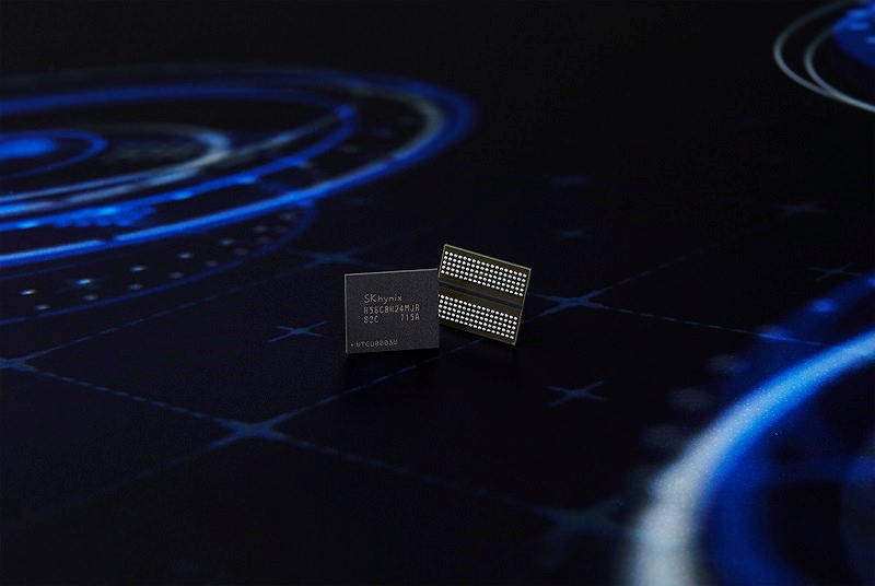
by Anton Shilov on April 30, 2017 11:00 AM ESTIn a surprising move, SK Hynix has announced its first memory chips based on the yet-unpublished GDDR6 standard. The new DRAM devices for video cards have capacity of 8 Gb and run at 16 Gbps per pin data rate, which is significantly higher than both standard GDDR5 and Micron's unique GDDR5X format. SK Hynix plans to produce its GDDR6 ICs in volume by early 2018.
GDDR5 memory has been used for top-of-the-range video cards for over seven years, since summer 2008 to present. Throughout its active lifespan, GDDR5 increased its data rate by over two times, from 3.6 Gbps to 9 Gbps, whereas its per chip capacities increased by 16 times from 512 Mb to 8 Gb. In fact, numerous high-end graphics cards, such as NVIDIA’s GeForce GTX 1060 and 1070, still rely on the GDDR5 technology, which is not going anywhere even after the launch of Micron's GDDR5X with up to 12 Gbps data rate per pin in 2016. As it appears, GDDR6 will be used for high-end graphics cards starting in 2018, just two years after the introduction of GDDR5X.
SK Hynix is not disclosing too many details about its GDDR6 chips, but they have revealed that the chips are 8 Gb devices with 16 Gbps data transfer rate, which in turn are being manufactured on SK Hynix's 21 nm process technology. The company is also stating that GDDR6 will have a 10% lower operating voltage than GDDR5, though they don't specify if that's relative to the low voltage (1.35 V), standard (1.5 V) or high frequency (1.55 V) version of GDDR5.
What is noteworthy is that SK Hynix does disclose some details about the first graphics cards to use its GDDR6 memory. As it appears, that adapter will have a 384-bit memory bus and will thus support memory bandwidth upwards of 768 GB/s. Given the number of chips required for a 384-bit memory sub-system, it is logical to assume that the card will carry 12 GB of memory. SK Hynix is not disclosing the name of its partner among GPU developers, but it is logical to assume that we are talking a high-end product that will replace an existing graphics card.
Unlike GDDR5X, GDDR6 is expected to be manufactured by all three major DRAM makers, and consequently should be available more widely. SK Hynix believes that GDDR6 will supplant both GDDR5 and GDDR5X relatively quickly. Nonetheless, keep in mind that while it took GDDR5 a relatively short amount of time to replace GDDR4 on high-end graphics cards in 2008 – 2009, it then took the memory standard years to replace GDDR3 on mainstream adapters.
Source: SK Hynix


28 Comments
View All Comments
osxandwindows - Sunday, April 30, 2017 - link
So, what about hbm?lilmoe - Sunday, April 30, 2017 - link
Soon (TM).ImSpartacus - Sunday, April 30, 2017 - link
HBM2 is already made by SK Hynix and Samsung. Sammy's HBM2 is used in Nvidia's GP100 and SK Hynix's HBM2 is used in Vega 10.But it looks like GDDR6 will provide 50% more bandwidth than the fastest GDDR5X sold today (which, itself, isn't even used at full speed in any of today's GPUs). So there won't be much of a reason for HBM2 to be used unless the exceptional efficiency is necessary. Otherwise, cheaper GDDR6 is probably preferred.
Flunk - Sunday, April 30, 2017 - link
AMD's RX Vega will have HBM2 and they still claim it will be released this quarter (Q2 2017).Frenetic Pony - Sunday, April 30, 2017 - link
HBM2 will show up in Vega "soon" whenever that is. Theoretically HBM can still scale beyond GDDR6 because its bandwidth is per die with multiple dies on a single GPU while DDR goes through its one bus. But that's also costly to have more and more dies, so GDDR6 is still quite competitive.At least until HBM3, which doubles the bandwidth again, comes along. Though who knows when that'll be out.
ImSpartacus - Monday, May 1, 2017 - link
Theoretically can't GDDR6 scale further as well?I mean, there's no physical law preventing a 512-bit setup, or, hell, a 768-bit setup.
Just like you can add more stacks in parallel, you can add more GDDR6 die in parallel.
fanofanand - Monday, May 1, 2017 - link
I could be mistaken but I think enlarging the bus is far more expensive than adding another die to the stack, and uses up a lot of power. There is a reason why Nvidia has almost always tried to go with a smaller bus.JasonMZW20 - Monday, May 1, 2017 - link
No physical law? Memory controllers take up die space, and you need extra transistors to run higher speeds. It's expensive. AMD had a 512-bit GDDR5 bus width in the 290(X)/390(X) to feed bandwidth hungry areas of the GPU (Hawaii), but AMD also succeeded in reducing its size in-die (vs Tahiti's 384-bit bus), albeit that came with a penalty in overall max RAM speed operation (5.5-6.0 Gbps).On top of that, you need to use more memory chips. Memory controllers are sets of dual-channel 64-bit (32x2) interfaces. To get the number of RAM chips you need, divide 512 by 32. So, you need 16 RAM ICs on the board.
512 = 16
384 = 12
256 = 8
768? That's 24 RAM chips. You'd have to clamshell (front and back of PCB) sets of 12. Still, a large PCB and power hungry even with the reductions in power consumption with GDDR6.
ImSpartacus - Sunday, April 30, 2017 - link
It sounds like GV102 will be using that 16ish Gbps GDDR6 on a standard 384-bit bus. That'll yield plenty of bandwidth. I wouldn't be surprised if actual speeds end up at like 14 Gbps initially. That'd still be plenty.And it's curious that they don't mention GV104. I wonder if it'll use 12 Gbps GDDR5X. That'd sync up with the recent rumors that GV104 is coming in Q3 2017 (too soon for GDDR6).
Dr. Swag - Sunday, April 30, 2017 - link
Yeah, nvidia seems to like 384 bit buses on their high end gpus, so my guess would be the product they're referring to would be gv102