AMD Radeon R9 285 Review: Feat. Sapphire R9 285 Dual-X OC
by Ryan Smith on September 10, 2014 2:00 PM ESTTonga’s Microarchitecture - What We’re Calling GCN 1.2
As we alluded to in our introduction, Tonga brings with it the next revision of AMD’s GCN architecture. This is the second such revision to the architecture, the last revision (GCN 1.1) being rolled out in March of 2013 with the launch of the Bonaire based Radeon HD 7790. In the case of Bonaire AMD chose to kept the details of GCN 1.1 close to them, only finally going in-depth for the launch of the high-end Hawaii GPU later in the year. The launch of GCN 1.2 on the other hand is going to see AMD meeting enthusiasts half-way: we aren’t getting Hawaii level details on the architectural changes, but we are getting an itemized list of the new features (or at least features AMD is willing to talk about) along with a short description of what each feature does. Consequently Tonga may be a lateral product from a performance standpoint, but it is going to be very important to AMD’s future.
But before we begin, we do want to quickly remind everyone that the GCN 1.2 name, like GCN 1.1 before it, is unofficial. AMD does not publicly name these microarchitectures outside of development, preferring to instead treat the entire Radeon 200 series as relatively homogenous and calling out feature differences where it makes sense. In lieu of an official name and based on the iterative nature of these enhancements, we’re going to use GCN 1.2 to summarize the feature set.
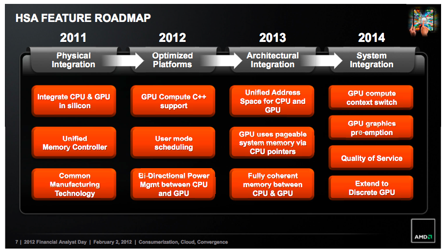
AMD's 2012 APU Feature Roadmap. AKA: A Brief Guide To GCN
To kick things off we’ll pull old this old chestnut one last time: AMD’s HSA feature roadmap from their 2012 financial analysts’ day. Given HSA’s tight dependence on GPUs, this roadmap has offered a useful high level overview of some of the features each successive generation of AMD GPU architectures will bring with it, and with the launch of the GCN 1.2 architecture we have finally reached what we believe is the last step in AMD’s roadmap: System Integration.
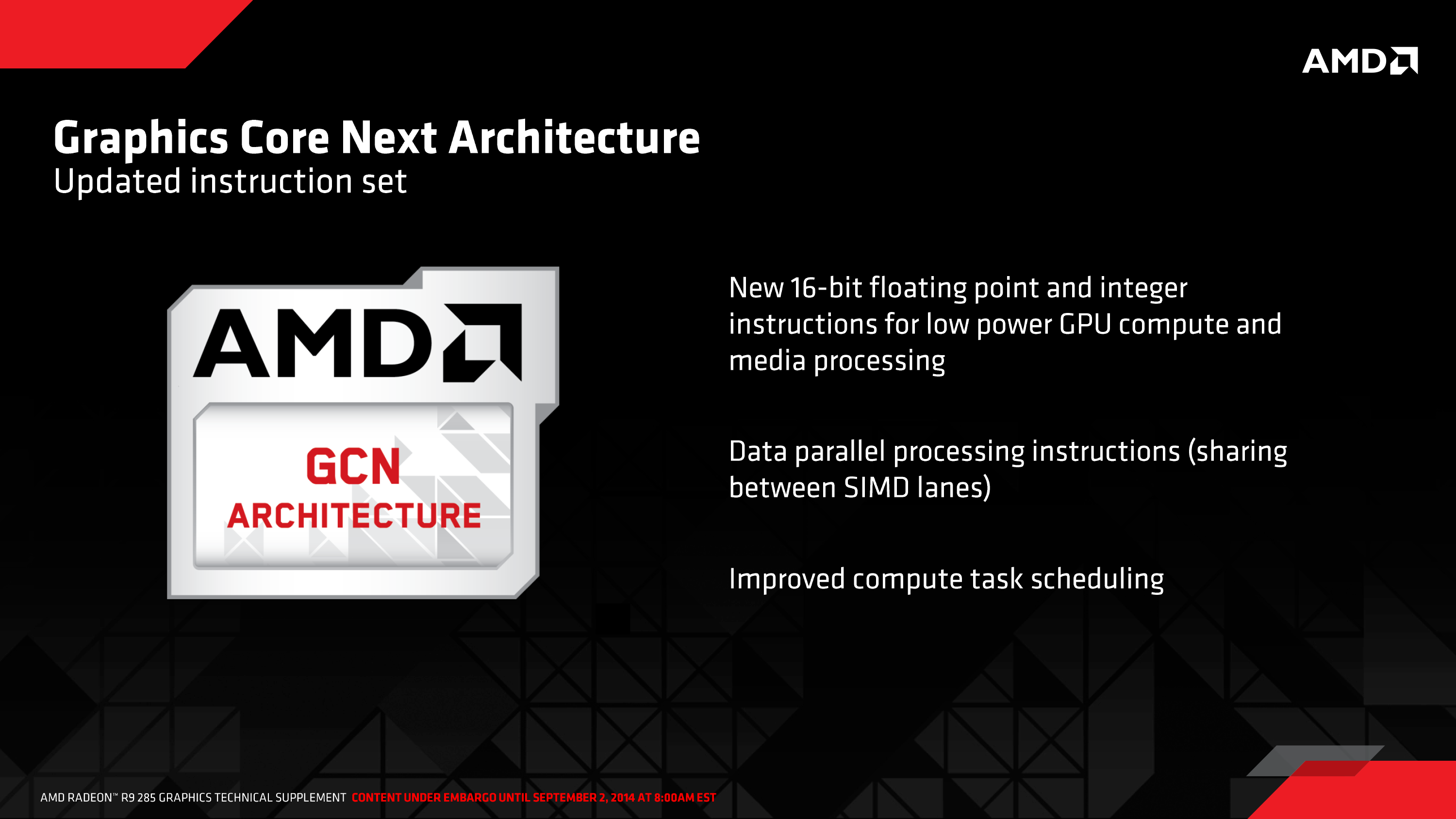
It’s no surprise then that one of the first things we find on AMD’s list of features for the GCN 1.2 instruction set is “improved compute task scheduling”. One of AMD’s major goals for their post-Kavari APU was to improve the performance of HSA by various forms of overhead reduction, including faster context switching (something GPUs have always been poor at) and even GPU pre-emption. All of this would fit under the umbrella of “improved compute task scheduling” in AMD’s roadmap, though to be clear with AMD meeting us half-way on the architecture side means that they aren’t getting this detailed this soon.
Meanwhile GCN 1.2’s other instruction set improvements are quite interesting. The description of 16-bit FP and Integer operations is actually very descriptive, and includes a very important keyword: low power. Briefly, PC GPUs have been centered around 32-bit mathematical operations for some number of years now since desktop technology and transistor density eliminated the need for 16-bit/24-bit partial precision operations. All things considered, 32-bit operations are preferred from a quality standpoint as they are accurate enough for many compute tasks and virtually all graphics tasks, which is why PC GPUs were limited to (or at least optimized for) partial precision operations for only a relatively short period of time.
However 16-bit operations are still alive and well on the SoC (mobile) side. SoC GPUs are in many ways a 5-10 year old echo of PC GPUs in features and performance, while in other ways they’re outright unique. In the case of SoC GPUs there are extreme sensitivities to power consumption in a way that PCs have never been so sensitive, so while SoC GPUs can use 32-bit operations, they will in some circumstances favor 16-bit operations for power efficiency purposes. Despite the accuracy limitations of a lower precision, if a developer knows they don’t need the greater accuracy then falling back to 16-bit means saving power and depending on the architecture also improving performance if multiple 16-bit operations can be scheduled alongside each other.
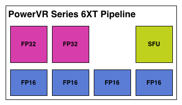
Imagination's PowerVR Series 6XT: An Example of An SoC GPU With FP16 Hardware
To that end, the fact that AMD is taking the time to focus on 16-bit operations within the GCN instruction set is an interesting one, but not an unexpected one. If AMD were to develop SoC-class processors and wanted to use their own GPUs, then natively supporting 16-bit operations would be a logical addition to the instruction set for such a product. The power savings would be helpful for getting GCN into the even smaller form factor, and with so many other GPUs supporting special 16-bit execution modes it would help to make GCN competitive with those other products.
Finally, data parallel instructions are the feature we have the least knowledge about. SIMDs can already be described as data parallel – it’s 1 instruction operating on multiple data elements in parallel – but obviously AMD intends to go past that. Our best guess would be that AMD has a manner and need to have 2 SIMD lanes operate on the same piece of data. Though why they would want to do this and what the benefits may be are not clear at this time.


86 Comments
View All Comments
chizow - Thursday, September 11, 2014 - link
If Tonga is a referendum on Mantle, it basically proves Mantle is a failure and will never succeed. This pretty much shows most of what AMD said about Mantle is BS, that it takes LESS effort (LMAO) on the part of the devs to implement than DX.If Mantle requires both an application update (game patch) from devs AFTER the game has already run past its prime shelf-date AND also requires AMD to release optimized drivers every time a new GPU is released, then there is simply no way Mantle will ever succeed in a meaningful manner with that level of effort. Simply put, no one is going to put in that kind of work if it means re-tweaking every time a new ASIC or SKU is released. Look at BF4, its already in the rear-view mirror from DICE's standpoint, and no one even cares anymore as they are already looking toward the next Battlefield#
TiGr1982 - Thursday, September 11, 2014 - link
Please stop calling GPUs ASICs - this looks ridiculous.Please go to Wikipedia and read what "ASIC" is.
chizow - Thursday, September 11, 2014 - link
Is this a joke or are you just new to the chipmaking industry? Maybe you should try re-reading the Wikipedia entry to understand GPUs are ASICs despite their more recent GPGPU functionality. GPU makers like AMD and Nvidia have been calling their chips ASICs for decades and will continue to do so, your pedantic objections notwithstanding.But no need to take my word for it, just look at their own internal memos and job listings:
https://www.google.com/#q=intel+asic
https://www.google.com/#q=amd+asic
https://www.google.com/#q=nvidia+asic
TiGr1982 - Thursday, September 11, 2014 - link
OK, I accept your arguments, but I still don't like this kind of terminology. To me, one may call things like fixed-function video decoder "ASIC" (for example UVD blocks inside Radeon GPUs), but not GPU as a whole, because people do GPGPU for a number of years on GPUs, and "General Purpose" in GPGPU contradicts with "Aplication Specific" in ASIC, isn't it?So, overall it's a terminology/naming issue; everyone uses the naming whatever he wants to use.
chizow - Thursday, September 11, 2014 - link
I think you are over-analyzing things a bit. When you look at the entire circuit board for a particular device, you will see each main component or chip is considered an ASIC, because each one has a specific application.For example, even the CPU is an ASIC even though it handles all general processing, but its specific application for a PC mainboard is to serve as the central processing unit. Similarly, a southbridge chip handles I/O and communications with peripheral devices, Northbridge handles traffic to/from CPU and RAM and so on and so forth.
TiGr1982 - Thursday, September 11, 2014 - link
OK, then according to this (broad) understanding, every chip in silicon industry may be called ASIC :)Let it be.
chizow - Friday, September 12, 2014 - link
Yes, that is why everyone in the silicon industry calls their chips that have specific applications ASICs. ;)Something like a capacitor, or resistor etc. would not be as they are of common commodity.
Sabresiberian - Thursday, September 11, 2014 - link
I reject the notion that we should be satisfied with a slower rate of GPU performance increase. We have more use than ever before for a big jump in power. 2560x1440@144Hz. 4K@60Hz.Of course it's all good for me to say that without being a micro-architecture design engineer myself, but I think it's time for a total re-think. Or if the companies are holding anything back - bring it out now, please! :)
Stochastic - Thursday, September 11, 2014 - link
Process node shrinks are getting more and more difficult, equipment costs are rising, and the benefits of moving to a smaller node are also diminishing. So sadly I think we'll have to adjust to a more sedate pace in the industry.TiGr1982 - Thursday, September 11, 2014 - link
I'm a longstanding AMD Radeon user for more than 10 years, but after reading this R9 285 review I can't help but think that, based on results of smaller GM107 in 750 Ti, GM204 in GTX 970/980 may offer much better performance/Watt/die area (at least for gaming tasks) in comparison to the whole AMD GPU lineup. Soon we'll see whether or not this will be the case.