The Haswell Review: Intel Core i7-4770K & i5-4670K Tested
by Anand Lal Shimpi on June 1, 2013 10:00 AM EST
This is a very volatile time for Intel. In an ARM-less vacuum, Intel’s Haswell architecture would likely be the most amazing thing to happen to the tech industry in years. In mobile Haswell is slated to bring about the single largest improvement in battery life in Intel history. In graphics, Haswell completely redefines the expectations for processor graphics. There are even some versions that come with an on-package 128MB L4 cache. And on the desktop, Haswell is the epitome of polish and evolution of the Core microprocessor architecture. Everything is better, faster and more efficient.
There’s very little to complain about with Haswell. Sure, the days of insane overclocks without touching voltage knobs are long gone. With any mobile-first, power optimized architecture, any excess frequency at default voltages is viewed as wasted power. So Haswell won’t overclock any better than Ivy Bridge, at least without exotic cooling.
You could also complain that, for a tock, the CPU performance gains aren’t large enough. Intel promised 5 - 15% gains over Ivy Bridge at the same frequencies, and most of my tests agree with that. It’s still forward progress, without substantial increases in power consumption, but it’s not revolutionary. We compare the rest of the industry to Intel’s excellent single threaded performance and generally come away disappointed. The downside to being on the top is that virtually all improvements appear incremental.
The fact of the matter is that the most exciting implementations of Haswell exist outside of the desktop parts. Big gains in battery life, power consumption and even a broadening of the types of form factors the Core family of processors will fit into all apply elsewhere. Over the coming weeks and months we’ll be seeing lots of that, but today, at least in this article, the focus is on the desktop.


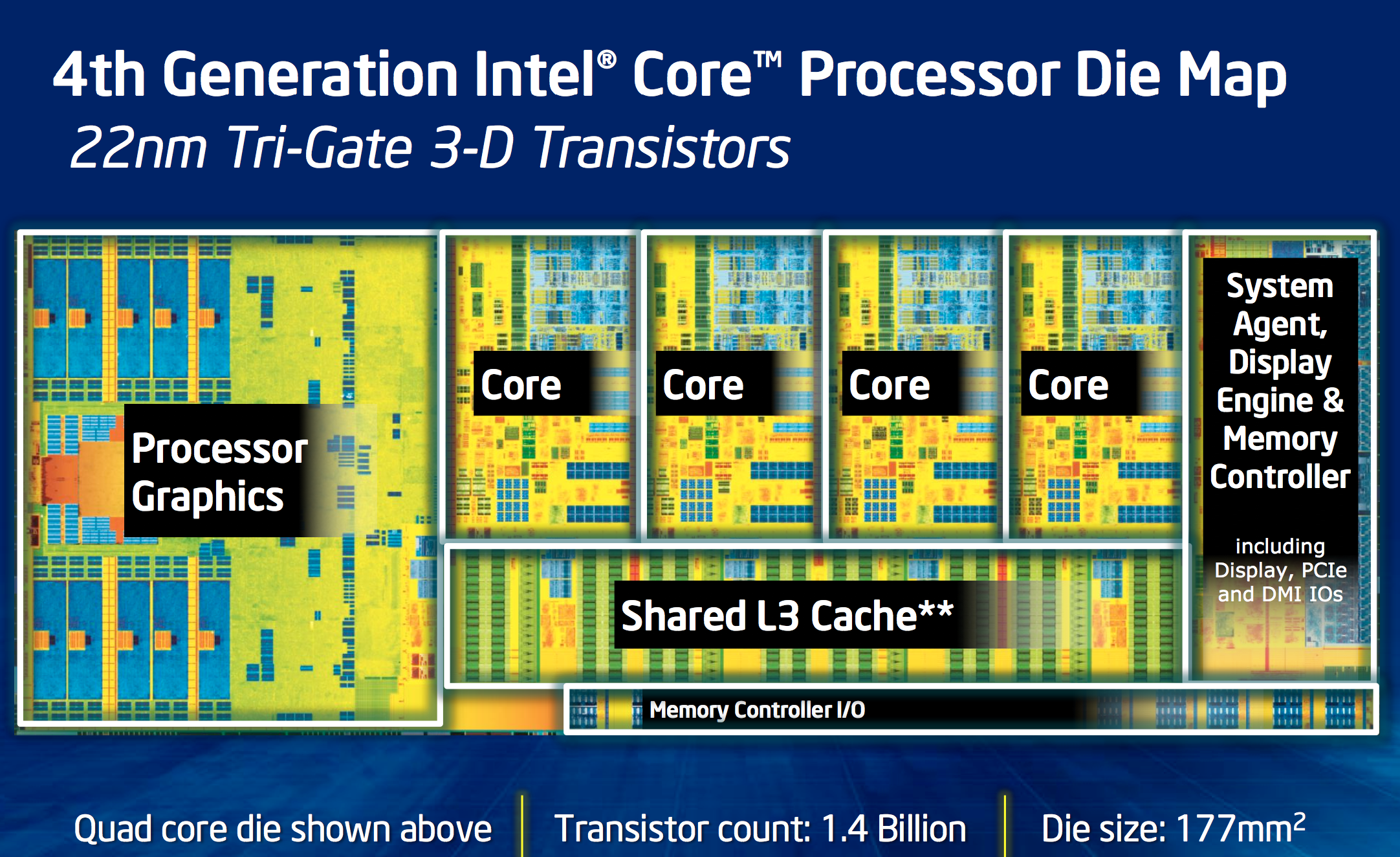
Haswell CPU Architecture Recap
Haswell is Intel’s second 22nm microprocessor architecture, a tock in Intel’s nomenclature. I went through a deep dive on Haswell’s Architecture late last year after IDF, but I’ll offer a brief summary here.
At the front end of the pipeline, Haswell improved branch prediction. It’s the execution engine where Intel spent most of its time however. Intel significantly increased the sizes of buffers and datastructures within the CPU core. The out-of-order window grew, to feed an even more parallel set of execution resources.
Intel added two new execution ports (8 vs 6), a first since the introduction of the Core microarchitecture back in 2006.
On the ISA side, Intel added support for AVX2, which includes an FMA operation that considerably increases FP throughput of the machine. With a doubling of peak FP throughput, Intel doubled L1 cache bandwidth to feed the beast. Intel also added support for transactional memory instructions (TSX) on some Haswell SKUs.
The L3 cache is now back on its own power/frequency plane, although most of the time it seems to run in lockstep with the CPU cores. There appears to be a 2 - 3 cycle access penalty as a result of decoupling the L3 cache.


210 Comments
View All Comments
chizow - Saturday, June 1, 2013 - link
Nice review Anand, it's pretty much what I expected from Haswell. 5-15% over IVB with all the bells and whistles of Lynx Point Z87 (6xSATA6G, more USB 3.0 etc.) This will make a nice upgrade for me coming from an OC'd i7-920 and X58 platform, now to see what deals MicroCenter has on the 4770K.I would have liked to have seen normalized clockspeed comparisons in the 5-gen Intel round-up but understand this does not reflect real-world results, given SB and above have much better turbo boost and base clocks. I think it would've given a better idea of IPC however, for those who have been overclocking their older platforms to similar max OC levels.
I also would have liked to have seen more gaming and OC'ing tests but understand this first review needed to cover most of the bases for a general audience, look forward to more testing in the future along with some looks at the Z87 chipset nuances.
Concillian - Saturday, June 1, 2013 - link
So what I'm seeing is 4770 compared with 3770... ~13% more power at load for Hasswell, but less than 10% more performance in the benchmarks? Is that correct?A5 - Saturday, June 1, 2013 - link
Anand's numbers put it at 13% faster with an 11% power increase. Not sure how you did the math.Concillian - Saturday, June 1, 2013 - link
You're right in that particular test. +12% power for +13% performance. Still disappointing. Most of the other benchmarks are showing less than 10% improvement, but we don't know the power story. Overall disappointing. With all the talk about power efficiency, I was hoping for +5-10% performance at the same or lower power consumption. All the power benefits seem to be at idle.gipper51 - Saturday, June 1, 2013 - link
I'm glad I went ahead and built my 3770 system a few months ago instead of holding out for Haswell. Nothing about Haswell was worth waiting for (for my needs). Damn...based on this and Intel's roadmaps I may be on IVB for a looooong time.LordSegan - Saturday, June 1, 2013 - link
Very weak new chip. Minimal increase in performance unless you are running a render farm or using a crappy ultra book. Useless for desktop gamers.vlvh - Saturday, June 1, 2013 - link
I'm just wondering what the rationalisation for using a Core 2 Duo for comparison benching is? Surely a Core 2 Quad (eg Q6600) would be a more accurate representation seeing as all the other parts in the benchmark are quad core.WhoBeDaPlaya - Saturday, June 1, 2013 - link
You'd think Anand would have covered something as important as this.I did not see this in _any_ of the reviews.
Also, the wording on the BCLK overclocking is a little odd. So bottom line - can we OC the 4770 using BCLK or not?
Kevin G - Monday, June 3, 2013 - link
The actual BLCK changes will be pretty much inline with what you'd be able to do on Z68 or Z77, about 110 Mhz max.Socket 1150 and Z87 add another bus multiplier to feed the CPU like socket 2011 parts have. So you can have a 100 Mhz clock feeding the PCI-E controller with a 1.25x multiplier a 125 Mhz clock will feed the CPU cores before the CPU multiplier. Increasing the BCLK to 108 Mhz and a 1.25 bus multiplier would equate to a 135 Mhz clock before the CPU multiplier is applied.
jmcb - Saturday, June 1, 2013 - link
All this means is when I finally get my first quad core PC, a 3770k will be cheaper. I see no reason to get this over that.