Qualcomm Announces Snapdragon 8 Gen 1: Flagship SoC for 2022 Devices
by Andrei Frumusanu on November 30, 2021 6:00 PM ESTMassive ISP Upgrades
I’ve been hearing for some time now that 2022 flagships will have massive camera upgrades, and the new features of the next-gen SoCs being described by MediaTek and now also Qualcomm explain why that is.
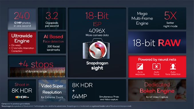
The new ISP of the Snapdragon 8 Gen 1 falls under a new marketing name – “Snapdragon Sight”, and includes large improvements of the capabilities of the IP blocks within the image processing chain.
The big flagship feature being advertised is the fact that the new ISP is now capable of 18-bits of color depth per channel, up from the previous generation 14-bit ISP. While mobile image sensors nowadays still are barely 12-bit native in terms of their ADCs, the ushering of new HDR techniques such as staggered HDR capture, where exposures are immediately subsequent to each other on the sensor’s readout, means that new phones now are able to capture images a lot faster, recombining them into higher bit-depth results. Particularly here, the new 18-bit ISP pipeline now allows for three exposure HDR stacking off these new sensors.
The increased bit-depth should allow for an increase of 4 stops in dynamic range (or 2^4 = 16x the range), which greatly helps with very contrasting environments and challenging lighting situations. This is quite beyond any other camera solution right now, and being able to have this implemented in such a hardware fashion sort of blurs the line between traditional image capture techniques and the more software-defined computational photography methods of the last few years.
Indeed, the new ISP architecture seems to be very much a way to implement many of the existing computational photography techniques into fixed-function blocks: there’s a new neural-net controlled 3AA (auto-exposure, auto-focus, auto-white-balance) and face detection block, which sounds eerily similar to Google’s HDRnet implementations.
Night mode is also said to be vastly improved through a new multi-frame noise reduction and image stacking block, being able to now stack and align up to 30 images, and achieve also much finer detail this generation. Qualcomm here claims up to 5x better night mode shots.
Further improvements include a new distortion correction block that’s able to now also correct for chromatic aberrations, and a hardware video Bokeh engine, being able to operate at up to 4K video recording. Think of it as the same as the new Cinematic mode on the new A15 iPhones, but not only limited to 1080p.
Qualcomm notes that all the AI/ML/neural network features on the ISP are actually run and accelerated on the ISP itself, meaning that it is not offloaded onto the Hexagon dedicated ML processing blocks or the GPU.
Just as a note- Qualcomm’s 3.2Gigapixel/s throughput metric here seems low compared to the Dimensity 9000’s 9Gpixel/s, it’s possible that the companies are advertising very different metrics, with MediaTek advertising the throughput of lower-bit depth pixels coming from the image sensors per frame, while Qualcomm quoting the full bit depth pixel processing within the ISP itself.
In terms of video encoders and decoders, the new chip allows for 8K HDR recording now, but otherwise is seemingly on par with the Snapdragon 888 media blocks. Unfortunately, this also means no AV1 decoding this year yet again. Qualcomm isn’t part of the Alliance for Open Media consortium and instead is backing VVC/H.266 and EVC, however with AV1 being actively pushed by Google and YouTube, and seeing large adoptions such as by Netflix, it’s becoming questionable for Qualcomm to still not support the format in 2022 devices.
AI Performance - Iterative, but solid
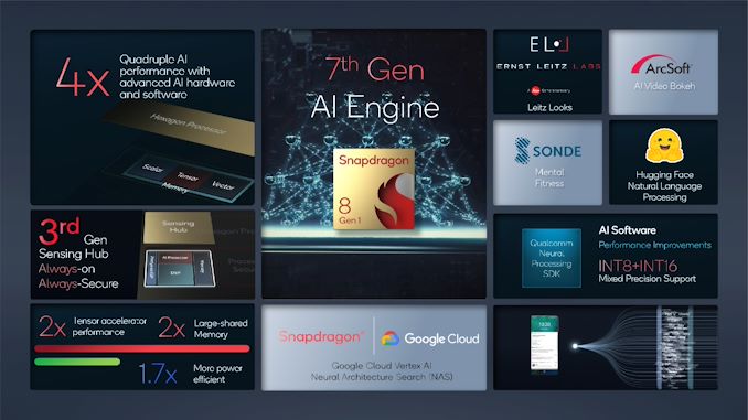
Last year’s Hexagon IP block was a very large change for the Snapdragon 888. At the time, Qualcomm moved on from a more segregated DSP/AI architecture to a single more fused-together block being able to operate on scalar, vector, and tensor operations at the same time. This year’s iteration is an improvement of that larger change. Qualcomm notes that amongst many changes, they’ve doubled up on the shared memory of the block, allowing for greater performance for larger ML models (which are growing at a very fast pace).
Qualcomm didn’t note any TOPS figures this time around, instead stating we’re seeing 2x the tensor throughput performance, and smaller increases for scalar and vector processing. They do quote a day-1 to day-1 performance increase of 4x when compared to the Snapdragon 888, via a combination of both hardware and software improvements, but of course that figure is smaller when comparing both platforms on an equal software footing.
Power efficiency for AI workloads is said to be 70% better this generation, which is actually more significant, and should help with more demanding sustained ML workloads.
X65 Modem Integrated
In terms of connectivity, the Snapdragon 8 Gen 1 is quite straightforward, as it integrates the X65 modem IP that Qualcomm had already announced as a discrete model earlier this year.
The improvements here are the fact that it’s a 3GPP Release 16 compatible modem, including new features such as uplink carrier aggregation. Other improvements are 300MHz of Sub-6 bandwidth on 3 100MHz carriers, and an increase of the mmWave bandwidth from 800 MHz to 1000MHz, allowing a new peak theoretical downlink speeds of 10Gbps.


219 Comments
View All Comments
BlueSwordM - Friday, December 3, 2021 - link
That's just Sisvel doing things their way.There hasn't been any legal or financial move, and I'm not aware of AV1 supporters actually paying the fees to it.
Adonisds - Tuesday, November 30, 2021 - link
I was sure they would add it this time. This is a huge disappointmentlinuxgeex - Wednesday, December 1, 2021 - link
The disappointing thing is lack of AV1 encode by all vendors in 2022, even on the desktop, even in the top-tier GPUs.dotjaz - Wednesday, December 1, 2021 - link
Are you stupid? Why are you disappointed by an impossible feature? Nobody expects AV1 HW encoder on a phone, at all. Nvidia will have some in 2022. It took Qualcomm 5 years to implement HEVC encoder. What makes you think 3 years for AV1 is possible?ksec - Wednesday, December 1, 2021 - link
Because that is what Open Media Alliance marketing promised. ( And failed to deliver )ChronoReverse - Wednesday, December 1, 2021 - link
Can you link the marketing slides with the promised arrival date of hardware encoders?ksec - Wednesday, December 1, 2021 - link
You should check out their original schedule of AV1 and delivering AV2 by "2020".ChrisGX - Wednesday, December 1, 2021 - link
Did they really promise AV1 encode capability in a mobile phone SoC? Commercial AV1 encoder ASICs, i.e. merchant silicon parts, are only just becoming available now. So far, even big players encoding content in AV1 have generally used software codecs running on high end CPU servers rather than specialised silicon developed in-house to get the job done.The following links point to a couple of products supplied by vendors of AV1 encoder ASICs as well as a broader range of issues around AV1 encoding of content and AV1 codecs.
https://www.prnewswire.com/news-releases/netint-an...
https://netint.ca/netint-announces-the-worlds-firs...
https://netint.ca/
https://www.design-reuse.com/news/50175/chips-medi...
https://www.wowza.com/blog/av1-codec-aomedia-video...
https://www.streamingmedia.com/Articles/Editorial/...
https://aomedia.googlesource.com/aom/
https://www.visionular.com/en/products/aurora1-av1...
name99 - Thursday, December 2, 2021 - link
HEVC was finalized in 2013Apple had working code on iPhone in 2014. (SW encode/decode, probably with some GPU assist).
Apple had full HW decoder in iPhone 2015.
Apple had full HW encoder in iPhone 2016.
But the HW was not really "visible" until iOS11 in 2017, when Apple made their big transition from "our preferred codecs are JPEG and h.264" to "our preferred codec is HEVC".
So
- HW encoder in 3 yrs *was* possible. Of course VVC is more complex than HEVC.
- chances are Apple will roll out a similar scheme -- experiment with (doubtless GPU-assisted) SW encode with current devices, ship a stealth HW decoder , then a stealth HW encoder, and maybe around 2024 transition their ecosystem to VVC (with two years of HW already in place, and a good enough SW solution for older HW).
BlueSwordM - Friday, December 3, 2021 - link
Actually, there is already a consumer level HW encoder...It is called the Nvidia Orin SOC.
I'm expecting Nvidia's next-gen GPUs to have AV1 HW encoding.