Intel's Process Roadmap to 2025: with 4nm, 3nm, 20A and 18A?!
by Dr. Ian Cutress on July 26, 2021 5:00 PM ESTSidebar on Intel EUV
In all of these announcements, one thing to highlight is Intel mentioning its relationship with ASML, the sole company that manufactures the EUV machines powering production of leading edge semiconductor manufacturing.
ASML is a unique company in that it is the only one that can produce these machines, because the technology behind them is often tied up with its partners and research, but also because all the major silicon manufacturers are heavily invested in ASML. For any other company to compete against ASML would require building a separate network of expertise, a decade of innovation and design, and a lot of capital. None of the major silicon vendors want to disturb this balance and go off on their own, lest it shuts them out of the latest manufacturing technology, and no research fund sees competing against the embedded norm as a viable opportunity. This means that anyone wanting EUV specialist technology has to go to ASML.
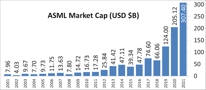
In 2012, it was reported that Intel, Samsung, and TSMC all invested in ASML. This was, at the time, to jumpstart EUV development along with migrating from 300mm wafers to 450mm wafers. While we haven’t moved to 450mm wafers yet (and there are doubts we will any time in the next decade), EUV is now here. Intel’s 2012 investment of $2.1 billion gave them a 10% stake in ASML, with Intel stating that it would continue investing up to a 25% stack. Those stakes are now below the 5% reporting threshold, but all three of the major foundry customers are still big owners, especially as ASML’s market cap has risen from $24 Billion in 2012 to $268 Billion in 2021 (surpassing Intel).
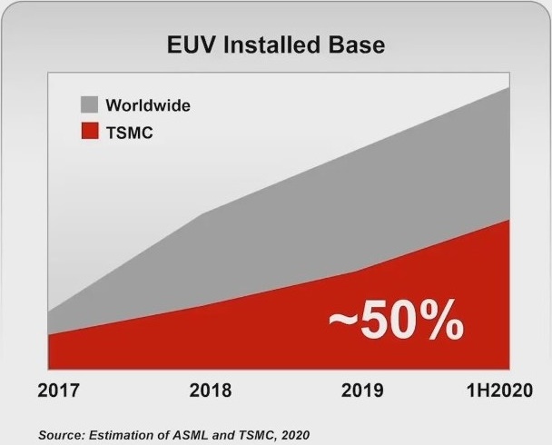
As major investors but also ASML’s customers, the race has been on for these foundries to acquire enough EUV machines to meet demand. TSMC reported in August 2020 that it has 50% of all EUV machines manufactured at ASML for its leading edge processes. Intel is a little behind, especially as none of Intel’s products in the market yet use any EUV. EUV will only intercept Intel’s portfolio with its new Intel 4 process, where it will be used extensively, mostly on the BEOL. But Intel still has to order machines when they need them, especially as there are reports that ASML currently has backorders of 50 EUV machines. In 2021, ASML is expected to manufacture around 45-50 machines, and 50-60 in 2022. The exact number of machines Intel has right now, or has ordered from ASML, is unknown. It is expected that each one has a ~$150m price tag, and can take 4-6 months to install.
With all that being said, Intel’s discussion point today is that it will be the lead customer for ASML’s next generation EUV technology known as High-NA EUV. NA in this context relates to the ‘numerical aperture’ of the EUV machine, or to put simply, how wide you can make the EUV beam inside the machine before it hits the wafer. The wider the beam before you hit the wafer, the more intense it can be when it hits the wafer, which increases how accurately the lines are printed. Normally in lithography to get better printed lines, we move from single patterning to double patterning (or quad patterning) to get that effect, which decreases yield. The move to High-NA would mean that the ecosystem can stay on single patterning for longer, which some have quoted as allowing the industry to ‘stay aligned with Moore’s Law longer’.
| ASML's EUV Shipments | |||||||||||||||||||||
| 2015 | 2016 | 2017 | 2018 | 2019 | 2020 | 2021 | |||||||||||||||
| Actual | 2 | 4 | 10 | 3 | 4 | 5 | 6 | 4 | 7 | 7 | 8 | 4 | 7 | 14 | 8 | 7 | 9 | - | - | ||
| Target (Total) | - | - | - | 20 (18) | 30 (26) | 35 (33) | 45-50 | ||||||||||||||
| 2018 and beyond is split per quarter for actual shipped numbers Data taken from ASML's Financial Reports |
|||||||||||||||||||||
Current EUV systems are NA 0.33, while the new systems are NA 0.55. ASML’s latest update suggests that it expects customers to be using High-NA for production in 2025/2026, which means that Intel is likely going to be getting the first machine (ASML NXE:5000 we think) in mid-2024. Exactly how many High-NA machines ASML intends to produce in that time frame is unknown, as if they flood the market, having the first won’t be a big win. However if there is a slow High-NA ramp, it will be up to Intel to capitalize on its advantage.


326 Comments
View All Comments
svan1971 - Monday, July 26, 2021 - link
why not just say 1nm in 2025 ? If your gonna lie, lie big or go homeishould - Monday, July 26, 2021 - link
Well, then Intel would win all silicon, game over, ggWaltC - Monday, July 26, 2021 - link
You know, Intel can't even hit 7nm yet--so there's no sense in discussing anything at all beyond that. He who makes the best products shall win the game--not so hard to understand, is it, Intel? I haven't seen an interesting architecture out of Intel yet! AMD has flashed by you as if you are sitting still...but hey--you are just sitting still, aren't you, Intel? Products talk--BS walks.RanFodar - Monday, July 26, 2021 - link
What kind of crap is this? You know Intel acknowledges their own faults now, and they're trying to remedy that with the first of these announcements. This node scheming is only for the purpose of realinging with the industry— and they're being more honest for that sake. Why not hold them to account to see if they're getting more and more competitive by the next few years?DigitalFreak - Monday, July 26, 2021 - link
Re-aligning with the industry? They're just making things up.persondb - Monday, July 26, 2021 - link
What are they making up? Their 10nm/7nm node is in the end about equal to TSMC and Samsung 7nmmode_13h - Monday, July 26, 2021 - link
Intel has been about as transparent as a brick wall. Their disclosures of schedule slip have been the bare minimum required by their customers and SEC reporting requirements. To this day, we still have zero visibility into exactly what went wrong. They've listed a bunch of leadership and organizational changes, but without insight into the root problems, it just amounts to: "trust us this time, for realz!"> Why not hold them to account to see if they're getting more and more competitive
> by the next few years?
Been there, done that. They've published similar roadmaps in the past, and they turned out to be worth less than the bits they were printed on.
Many years late, Intel did manage to get 10 nm products into end users' hands, followed by 10 nm SFF. So, they haven't lost *all* credibility. We can expect them to deliver on most of their promises *eventually*. It's mainly just a question of which decade.
Kevin G - Tuesday, July 27, 2021 - link
Intel hasn't disclosed what went wrong but looking at what the other fabs have done it should be pretty evident: they went with EUV sooner and were not as aggressive pursuing peak density. Intel's 10 nm process was a quad pass, self aligned schema that is seemingly too complex for mass production. The super fin and enhanced super fin advancements sacrificed that absolute density in favor of getting a working node.EUV is a great reset on as it reduces the need for multi-pass layers. This is also why Intel does have a legit chance in surpassing the other foundries with high-NA by securing these next generation ASML machines before their competitors. If the competition doesn't have these same tools at the same time as Intel, it is a clear technological advantage. The real question is how much money did it take to secure that deal.
mode_13h - Wednesday, July 28, 2021 - link
> they went with EUV soonerUh, no. I thought they were *late* to the EUV party and got themselves in a position of having to wait in line to get EUV machines. The article is consistent with this.
> were not as aggressive pursuing peak density.
I heard their 10 nm was too high-density, and that was part of the problem. From the chart on page 1, it's certainly claimed to be higher-density than TSMC 7 nm.
> EUV is a great reset on as it reduces the need for multi-pass layers.
I thought EUV requires more passes, which is one reason it's more expensive.
Spunjji - Thursday, July 29, 2021 - link
@mode_13h - I think Kevin G meant Intel's *competitors* went with EUV sooner, not Intel - hence also them not aggressively pursuing peak density, which is not something Intel could be accused of...EUV reduces the number of passes required, because less (or no) multi-patterning is required to reach the same density as a process using DUV. The problem you're likely thinking of is that EUV machines are still in a state where each pass through them is slower than through a DUV machine due to relatively weak beam intensity, and the masks have to be handled with greater care (no pellicles) and replaced more often.
Presumably Intel thought they would be better off sweating existing known-good assets than trying to figure out how to integrate relatively experimental tech into an entirely new workflow. They lost that bet.