Qualcomm Announces Snapdragon 865 and 765(G): 5G For All in 2020, All The Details
by Andrei Frumusanu on December 4, 2019 1:50 PM EST- Posted in
- Mobile
- Qualcomm
- Smartphones
- SoCs
- 7nm
- 5G
- Snapdragon 865
- Snapdragon 765
Cortex-A77 Cores, LPDDR5, Adreno 650 GPU
No More CPU Customisations For Now: Cortex-A77 Used
On the CPU side, the Snapdragon 865’s improvements over the Snapdragon 855 are very straightforward in terms of specifications:
| SoC |
Snapdragon 865 |
Snapdragon 855 |
| CPU | 1x Cortex A77 @ 2.84GHz 1x512KB pL2 3x Cortex A77 @ 2.42GHz 3x256KB pL2 4x Cortex A55 @ 1.80GHz 4x128KB pL2 4MB sL3 @ ?MHz |
1x Kryo 485 Gold (A76 derivative) @ 2.84GHz 1x512KB pL2 3x Kryo 485 Gold (A76 derivative) @ 2.42GHz 3x256KB pL2 4x Kryo 485 Silver (A55 derivative) @ 1.80GHz 4x128KB pL2 2MB sL3 @ 1612MHz |
We find the same 1+3+4 CPU configuration as found on the Snapdragon 855, using the same 2.84GHz, 2.4GHz and 1.8GHz clock frequencies, and the same 512KB, 256KB and 128KB L2 cache configurations.
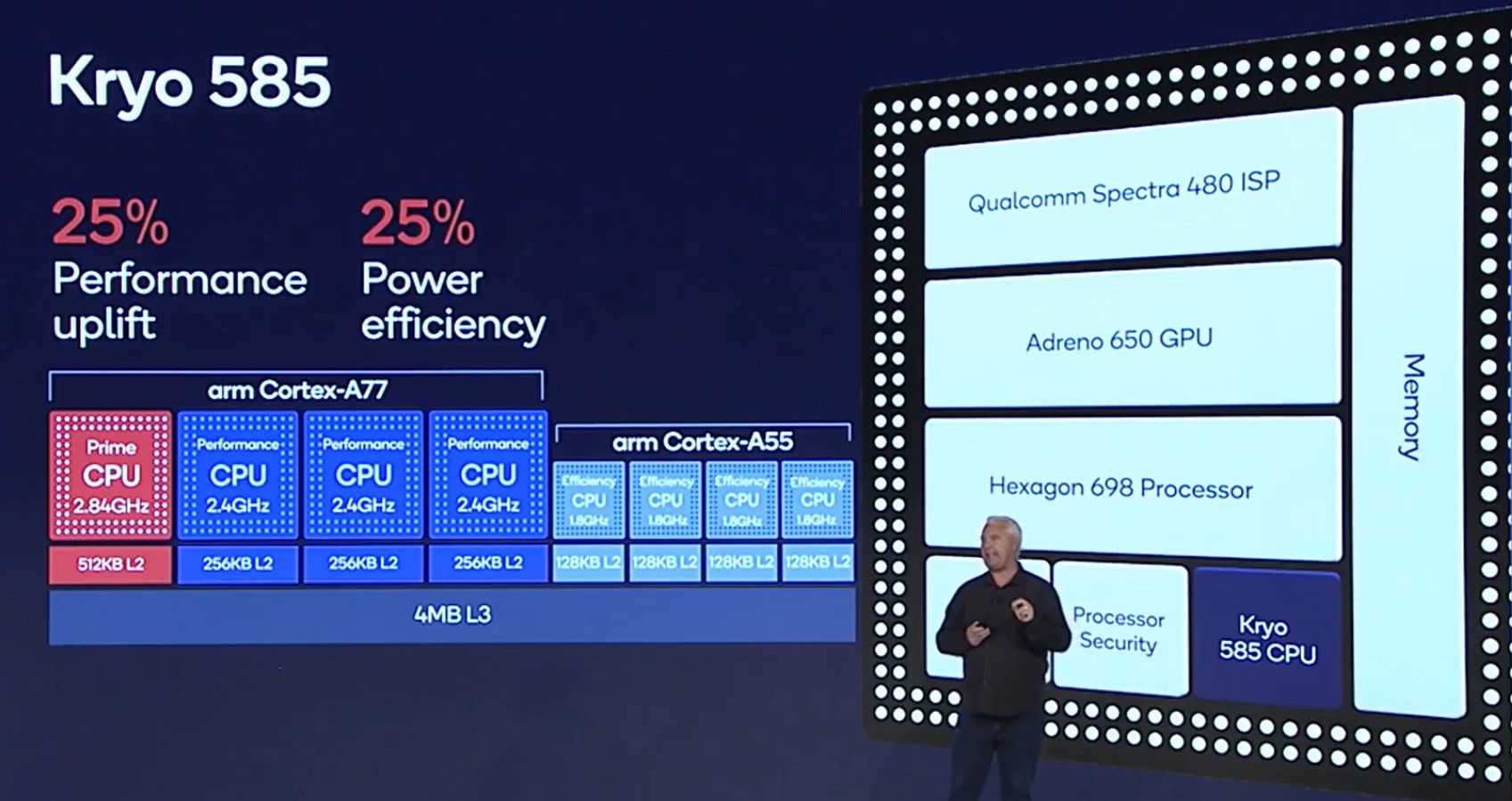
The big difference of course, that instead of using Cortex-A76 based cores in the S855, the new chipset is using Arm’s newest Cortex-A77 cores. A larger change in strategy this year is that while Qualcomm still uses the “Built-on-Cortex-technology” license to be able to customize some parts of the interface IP of the CPUs (And be able to brand it as the Kryo 585 parts), they’ve abandoned customisations on the CPU core itself. Qualcomm saw that the return on time investment with Arm to customise previous generations didn't result in as high returns as they would have hoped, and for the Snapdragon 865 they simply opted to use the default configuration Cortex-A77 as offered by Arm.
Still, the new CPU microarchitecture is said to be able to offer a 25% performance uplift this year, all of it which is essentially due to IPC improvements of the new design. As we had expected, we’re not seeing any clock improvements this year, and the CPU frequencies remain flat, reaching an identical 2.84GHz for the “Prime” core and 2.4GHz for the “Gold” cores.
Qualcomm claims a 25% power efficiency gain for the new SoCs, but this is an ISO-performance comparison against the previous generation (At equal performance to the S855, the S865 uses 25% less energy/power). In absolute terms at maximum performance, the new Snapdragon 865 big CPUs use more power to achieve their higher performance, meaning efficiency at peak perf is flat.
The Cortex-A55 cores remain practically the same, which to be honest are getting a bit long in the tooth as they’ve essentially not changed in 3 generations now. We’re very much overdue a large microarchitectural update from Arm as the yearly small efficiency core updates from Apple now put the Android SoCs to shame in regards to performance and efficiency.
One aspect that Qualcomm did finally improve on is the L3 cache of the CPU cluster, which has now been increased from 2MB to 4MB. While the performance benefits here are welcome, Qualcomm explains that the main reason for the change was increased power efficiency, reducing more expensive DRAM memory accesses in light workloads, which makes a lot of sense.
The Adreno 650 GPU: Similar Architecture, Wider Microarchticture
On the GPU side of things, we’re seeing Qualcomm make evolutionary changes to the new IP block. It’s actually a bit unusual for Qualcomm to remain in the 600-series this year and the company had never before stretched out an architecture over three generations like this.
| SoC |
Snapdragon 865 |
Snapdragon 855 |
| GPU | Adreno 650 @ ? MHz +25% perf +50% ALUs +50% pixel/clock +0% texels/clock |
Adreno 640 @ 585 MHz |
Qualcomm’s improvement claims for this generation come down to an aggregate of 25% over a variety of industry benchmarks and real workloads. It’s to be noted that the company did say we’ll be see higher improvements in some workloads, for example higher complexity tests such as Aztec might see a higher percentage.
Qualcomm's "Mobile GPU approaches to power efficiency"
@ High-Performance Graphics 2019
Earlier last summer Qualcomm did detail some titbits of its architecture, describing the ALUs execution units as being separate MUL+ADD units per lane, and also showcased some first-party performance metrics of the Adreno 640 GPU. The Adreno 630 and 640 were both 2-core GPUs with each respectively 256 and 384 ALUs per core based on the measured throughput. The Adreno 650 increasing this by 50% could either mean we’re seeing three 256-ALU cores, or that there’s now two 512-ALU cores. The resulting computational power at a hypothetical 600MHz clock rate would be ~1.2TFLOPs. We’ll have to wait and see where the frequency ends up at, Qualcomm didn't want to disclose it.
The Adreno 640 had made a huge jump in texture fillrate as it doubled up from the TMUs from 12 per core to 24 per core, for a total of 48. This resulted in quite the unusual 3:1 texel:pixel ratio in terms of fillrate capability. The Adreno 650 now increasing the ROPs by 50% means well see an increase from 8 per core (16 total) to 12 per core (24 total), bringing it back to a 2:1 balance, with the pixel fillrate capabilities now catching up to the Mali GPU counterparts.
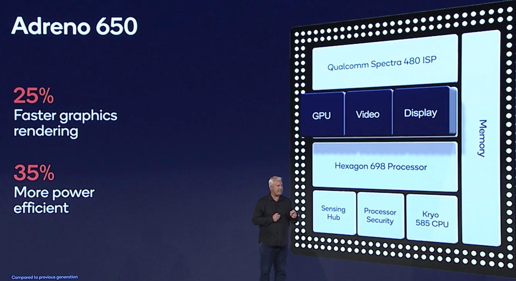
I asked about absolute power consumption, and the company discloses that it’ll be similar to the Snapdragon 855 in terms of peak power. There’s a slight contradiction here as the company also mentions that sustained performance is going to be a lot better than on the S855. It’s possible that we would be seeing larger performance improvements at lower than peak frequencies, and the company does say that at equal performance levels, the Adreno 650 is now 35% more efficient than its predecessor.
It was also a good opportunity to talk about the increasing peak power consumption over the last few generations. Back during the Snapdragon 835 days and earlier, Qualcomm’s SoCs were praised and took pride in being able to remain quite cool, with peak device active load power only being 3.5-4W. In more recent generations this has steadily increased, with the Snapdragon 855 now falling in at around 5W. Qualcomm explains that this was actually a change requested by OEMs who had improved the thermal dissipation capabilities of their device designs – telling the company that they are now able to handle higher power levels, and for Qualcomm to use that to increase performance.
I’m not too sure how to feel about this as it’s pretty much a double-edged sword and puts the responsibility of actually achieving the peak performance of the SoC solely in the hands of the device vendor, and them being able to properly design a good thermal solution. As we’ve already seen this year, some vendors are doing well in this regard, while others prioritise temperature over retaining higher performance levels. In any case, our unique testing methodology makes sure we’re exposing such differences in detail.
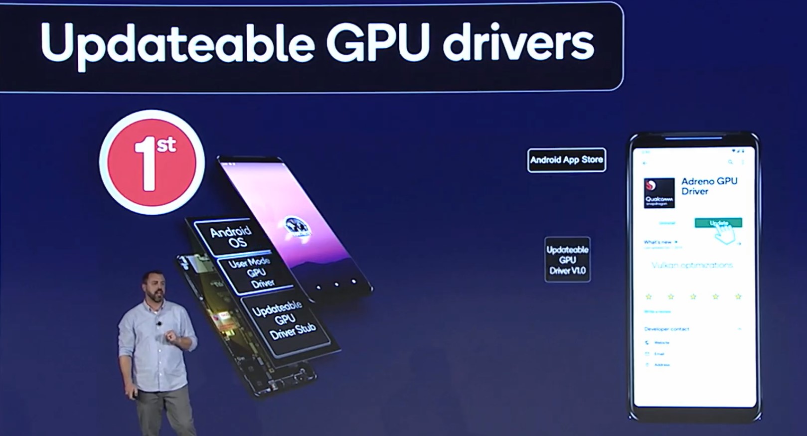
Unrelated to the hardware of the GPU, a big new improvement for the Adreno 650 and Snapdragon SoCs going forward is the fact that Qualcomm is now planning to distribute and update the graphics drivers over the Play Store. This feature was actually introduced to Android back in 2017 with Android 8/Oreo, but up until now no vendors actually ever took advantage of it, as it looks like it took time for vendors to make this feature operable with their BSPs. Qualcomm is now the first to achieve this, and the company is planning on quarterly GPU driver updates for new SoC generations going forward.
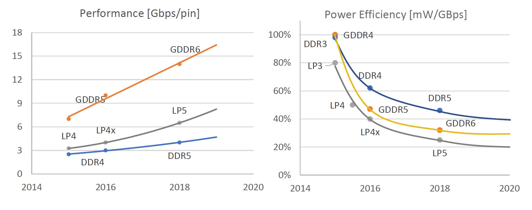
2020 Sees The Commercialisation of LPDDR5
2020 is the year where we’ll be seeing LPDDR5 being introduced to mobile. The new memory standard promises to improve the power efficiency per bit transferred by roughly 20%, and the Snapdragon 865 now comes with support for the new technology.
| SoC |
Snapdragon 865 |
Snapdragon 855 |
| Memory Controller |
4x 16-bit CH @ 2133MHz LPDDR4X / 33.4GB/s or @ 2750MHz LPDDR5 / 44.0GB/s 3MB system level cache |
4x 16-bit CH @ 2133MHz LPDDR4X 33.4GB/s 3MB system level cache |
What’s interesting here is that Qualcomm is using a hybrid memory controller, supporting both LP4X and LP5 memory standards. LPDDR4X is supported to up to 2133MHz, while LPDDR5 memory is supported 2750MHz (5500MHz effective considering DDR). The bandwidth improvement here is 31%, and Qualcomm notes that the two technologies will roughly offer the same memory latency, meaning no improvement nor degradation.
Surprisingly, Qualcomm sounded rather conservative in regards to the actual performance impact of the new technology. They do say that it will bring advantages in bandwidth starved situations, but the company’s representatives underplayed the impact that it will have. Qualcomm allows vendors to choose between LP4X and LP5 in their device implementations, and says the performance differences between the two would a few percentage points. The new memory technology is rather a matter of future-proofing the SoC as well as being able to support the memory as DRAM-manufacturers shift their production lines.
The company also said that they’ve improved the memory subsystem of the SoC and were able to lower latency to around “130ns”, although it’s not exactly clear what the context and percentage improvement here is – if it’s most likely a full random access test, in which case in comparison the S855 landed in at 150-170ns depending on memory depth, then that’s actually a quite notable and respectable improvement.
The system level cache of the SoC still falls in at 3MB this generation, the same as the previous generation. I questioned if it made sense to still maintain this at this size, especially in the face of now almost every vendor having a similar capability, and especially in the face of Apple’s humongous 16MB implementation in the A13. The company said that for their architecture and workloads that they’re seeing, they opted to retain the size, but are looking into the future to possibly increase it (Die area is probably a large consideration here, maybe expect an increase in the next process node?).


91 Comments
View All Comments
name99 - Wednesday, December 4, 2019 - link
Andrei, something I asked last year, but never got an answer --- maybe this year QC will tell us:- is the fast core actually different from the slow cores in that it's using faster transistors? Or could the slow cores equally well be clocked at 2.84GHz if QC policy allowed it?
Or to put it differently, what's the energy excess for solving a problem at 2.84GHz rather than at 2.42? Is the slope so steep that running more than one core that fast was utterly infeasible?
(Point is, if it's the same transistors, so all cores could clock to 2.84, then it's usual quadratic overhead. But if the 2.84 circuits use HP rather than HE/HD transistors, the energy excess could be quite a bit higher.)
Kabm - Wednesday, December 4, 2019 - link
In the past QC give the one fast core more cache too. Energy aside, if they use all fast cores and a core failed that speed then the whole soc is failed, more cost overallRaqia - Wednesday, December 4, 2019 - link
The transistors used on the prime core have a larger pitch and use more fins:https://fuse.wikichip.org/news/2408/tsmc-7nm-hd-an...
name99 - Thursday, December 5, 2019 - link
Thanks! Great link.Andrei Frumusanu - Thursday, December 5, 2019 - link
It's a physically different core.Dragonstongue - Wednesday, December 4, 2019 - link
I still not quite understand why they have not really bothered to have true LOW - Mid - HIGH speed for the whole bunch of cores, I imagine would not be "that hard" would keep power use in check big time as well (save battery life, as pretty much all phone makers these days only want to sell a SEALED phone..let them play their game, let us enjoy what we have as long as possible)example
top core at whatever Ghz range, the mid cores at 1/2 to 1/3 less than this, the low cores (have maybe more of) but 1/2 the mid speed
so (again example)
1 @ 2.84Ghz
3 @ 1.42 or 1.89
4 @ 710Mhz or 945Mhz
I am quite certain with the "tweaking" they do and have done (for a number of years now)
even at say 500Mhz on 4 cores, it will still be able to handle many many things "just fine" provided they work their magic so it feeds and is fed by the memory and/or graphics properly
heck, they might even be able to use the good chunk extra power drop to clock the graphics up so even though it ends up using LESS power (stays very cool as well) still feels snappy as lightning
We have the technology, why not use it far more "intelligently" I ask?
peevee - Friday, December 6, 2019 - link
"We have the technology, why not use it far more "intelligently" I ask?"Total MT performance IN TESTS of your 1+3+4 configuration would be significantly lower than current 1+3+4 configuration, and review sites still insist on publishing irrelevant numbers.
The best configuration would probably be 1 superfast+16 superefficient.
Kabm - Wednesday, December 4, 2019 - link
Quote: "We also expect some compromises in terms of battery efficiency due to the silicon overhead, however as a counter-argument, Apple’s iPhones always have had separate AP+modem solutions, and the latest generation this year had amongst the strongest battery life performance of any device out there, even with a competing Intel modem."No you tested iPhone on wifi without 4G usage so cannot say it had strong battery life in 4G or 5G.
yacoub35 - Thursday, December 5, 2019 - link
>Qualcomm says this would be possible if you essentially just ignore the X55’s 5G capabilities, but they don’t see any reason for any vendor to actually do this. In essence, bar any abnormal decision from some vendors, all Snapdragon 865 devices in 2020 will be full 5G devices.I'll definitely take the one without the cellular equivalent of a cancer stick embedded in it (5G).
peevee - Friday, December 6, 2019 - link
There is a non-zero probability that mmWave in phones will be prohibited in 10 years. Not that anybody would really miss it as it does not work in real-life situations anyway (does not even penetrate your head/body, just warms and/or injures it).