Intel's Architecture Day 2018: The Future of Core, Intel GPUs, 10nm, and Hybrid x86
by Dr. Ian Cutress on December 12, 2018 9:00 AM EST- Posted in
- CPUs
- Memory
- Intel
- GPUs
- DRAM
- Architecture
- Microarchitecture
- Xe
Sunny Cove Microarchitecture: A Peek At the Back End
One of the best parts when a new microarchitecture is announced is learning how it all works and how it has changed. Intel has been on close variants of the Skylake core since Skylake first launched in 2015, which has carried through Kaby Lake, Coffee Lake, and Coffee Lake refresh – and so getting an update to his old core design is more than welcome. While I applaud Intel for getting something new to put in front of our faces, the level of information was unfortunately less than complete. For reasons of ‘we’ll discuss more nearer the launch’, Intel was only set on discussing the back end of the microarchitecture design in any detail. In core design parlance, this means everything beyond the dispatch and order queues.
Intel framed its microarchitecture updates into two different sections: general purpose performance increases and special purpose performance increases. The company described the general purpose updates essentially as raw IPC (instructions per clock) throughput or an increase in frequency. An increase in either of these two leads to a performance increase no matter the code, at least as long as it is compute bound. Frequency is often a function of the implementation and process, whereas IPC increases can come from cores being wider (more executing instructions per clock), deeper (more parallelism per clock), and smarter (better data delivery through the front end).

The other type of performance increase is the special purpose kind, which means that certain workloads used in specific scenarios can be improved through additional acceleration methods, such as dedicated IP or specialized instructions.
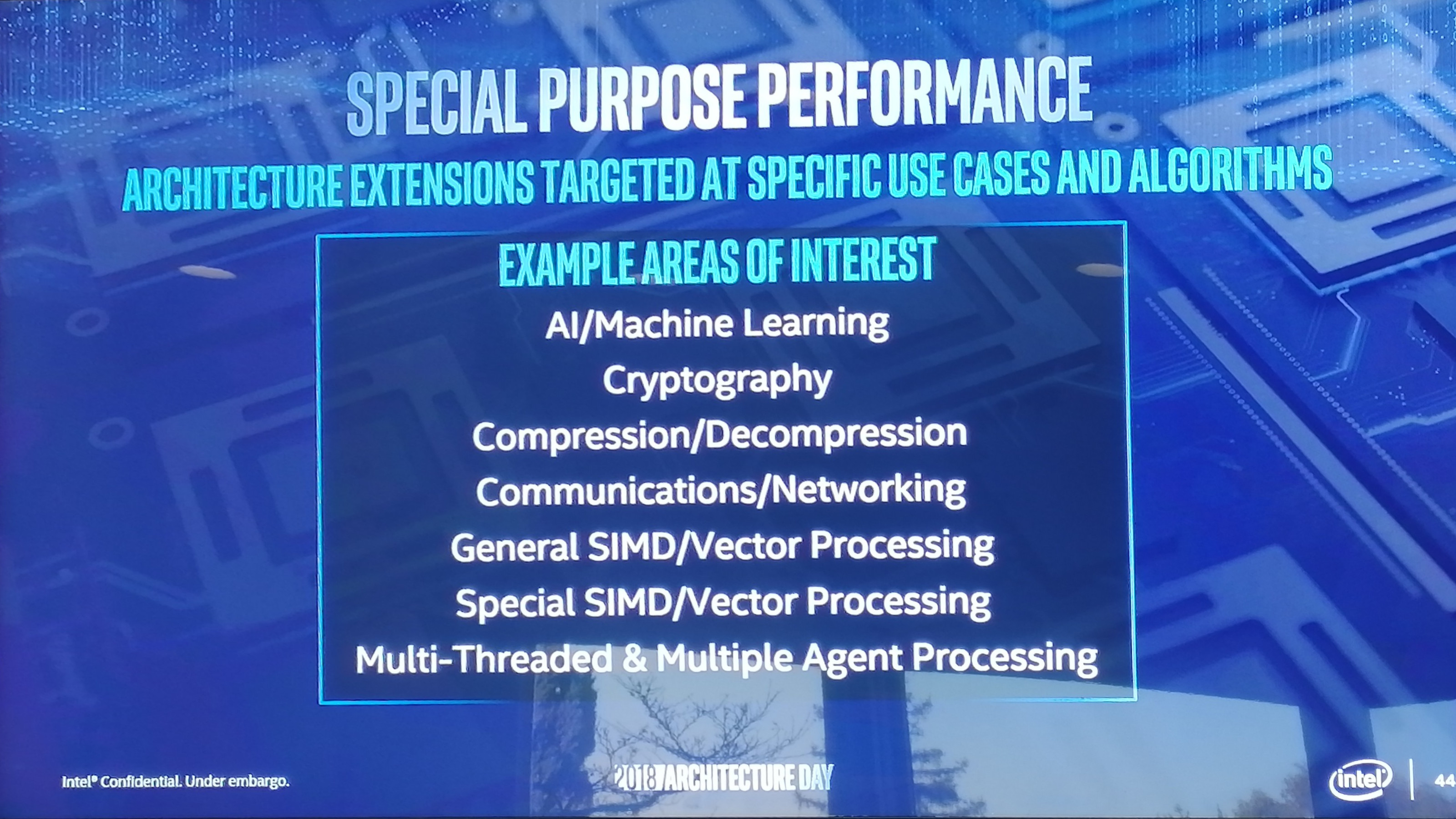
Sunny Cove is set to have both.
On the back end of the microarchitecture design, Intel has done several things including increasing cache sizes, making the execution of the core wider, increasing L1 store bandwidth, and other things.
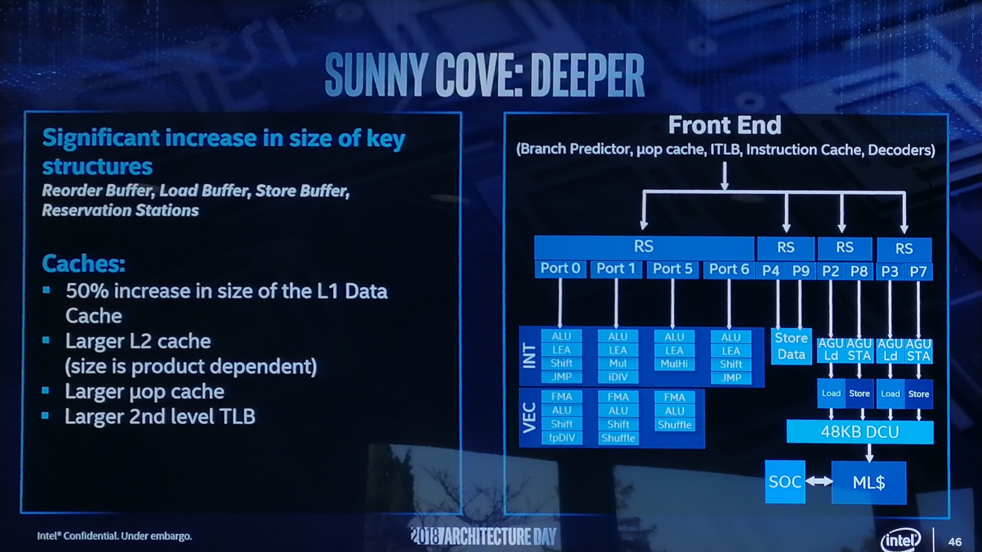
Starting with the cache improvements, the Sunny Cove core back end has a 48 KB L1 Data cache, upgraded from 32 KB. Normally cache misses decrease by a factor of a square root of the proportional size when the cache is increased, so in this case we should expect a 22% reduction in L1-Data cache misses. We are told that the L2 cache size has also been increased in both the Core and Xeon variants of Sunny Cove (256 KB and 1 MB respectively), although to exactly what size will be revealed at a later date.
While not back-end, the micro-op (uOp) cache has increased from a 2048-entry design, although exactly to what Intel is not saying at this point. The second level TLB size has also increased, which will help with machine address translation of recent addresses – normally this is increased when more lookups need to be kept and stored, which means that Intel identified a number of use cases where recent addresses had been evicted shortly before being needed.

From the diagram we can see some other changes, such as the increase in execution ports from eight to ten, allowing more instructions to come out of the schedulers at one time. Port 4 and Port 9 is linked to a cycling data store, doubling that bandwidth, but also the AGU store capabilities have doubled, for which the increased L1-D size will help. Previously on Skylake there was a potential bottleneck when all three AGUs could attempt a store, however only enough bandwidth was present for one per clock cycle. Load performance is unaffected. There is also an allocation increase, moving from four to five. This means that the dispatch out of the reorder buffer can now hit five instructions per cycle, rather than four – however given that the ops/cycle out of the Skylake decoders and uOp cache was four-to-five (depending on certain factors), it will be interesting to see how the front end has changed as a result.
There are also substantial changes in the execution ports between Skylake and Sunny Cove, which is best represented in a diagram and a table:
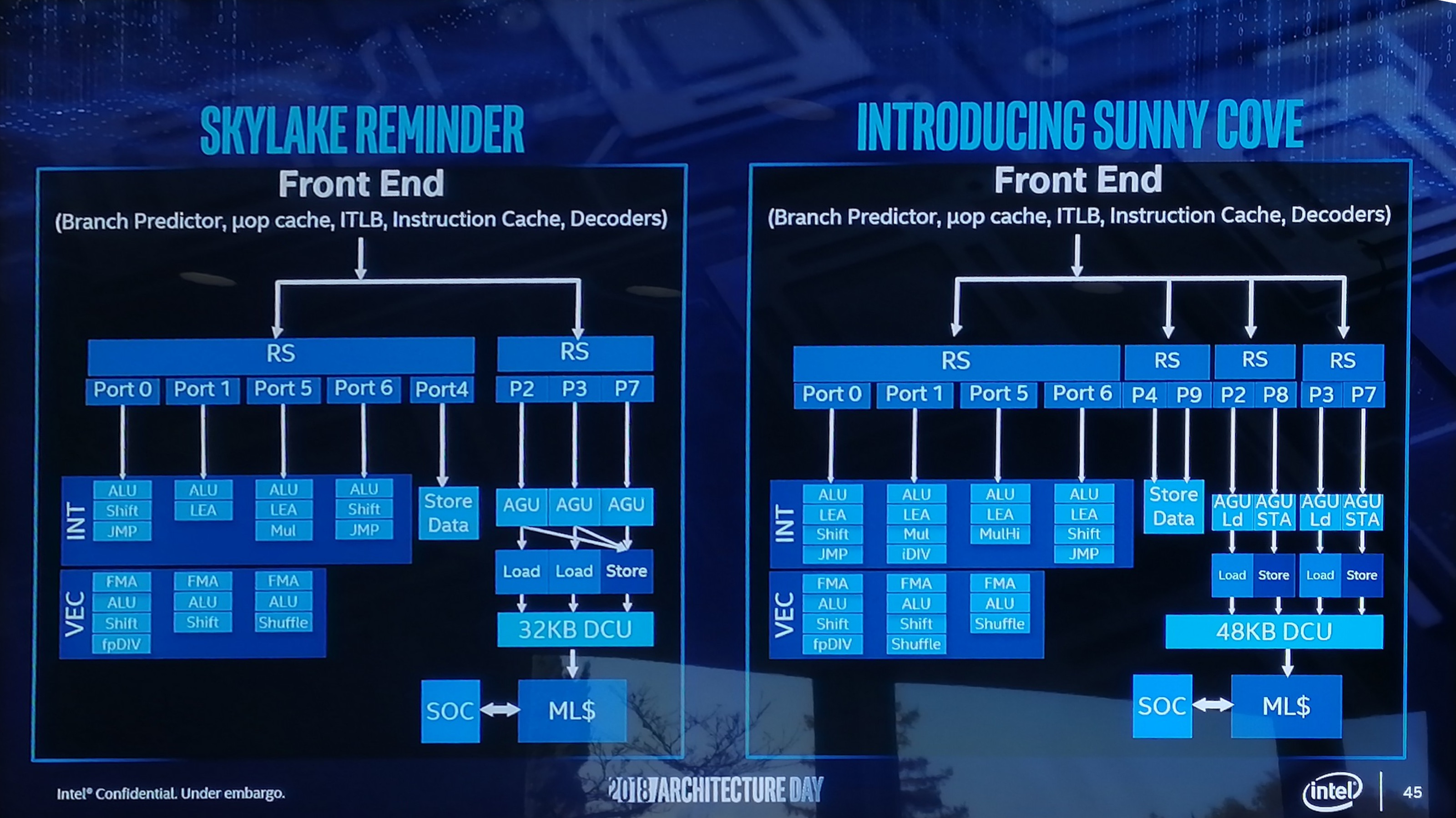
| Back-End Execution Resources | ||||||||
| Skylake | Port | Sunny Cove | ||||||
| Integer | ||||||||
| JMP | Shift | ALU | 0 | ALU | LEA | Shift | JMP | |
| LEA | ALU | 1 | ALU | LEA | Mul | iDIV | ||
| Mul | LEA | ALU | 5 | ALU | LEA | MulHi | ||
| JMP | Shift | ALU | 6 | ALU | LEA | Shift | JMP | |
| Vector / FP | ||||||||
| fpDIV | Shift | ALU | FMA | 0 | FMA | ALU | Shift | fpDIV |
| Shift | ALU | FMA | 1 | FMA | ALU | Shift | Shuffle | |
| Shuffle | ALU | FMA | 5 | FMA | ALU | Shuffle | ||
The parts highlighted in bold are different in the Sunny Cove core.
We see that Intel has equipped the Integer section of the core with more LEA units to help with memory addressing calculations, possibly to help improve performance loss with security mitigations that require frequent memory calculations or to help with high-performance array code with constant offsets. Port 1 gets the Mul unit from Skylake Port 5, probably for rebalancing purposes, but there is also an integer divider unit here. This addition is a bit of a tweak, as we know that Cannon Lake has a 64-bit IDIV unit in its design as well. In that case it brings 64-bit integer division down from 97 clocks (a mix of instructions) down to 18 clocks, and this is likely something similar. Also on the INT side is that Port 5’s multiply unit has become a ‘MulHi’ unit which in other implementations leave most-significant nibble of the result in a register for further use. I'm not sure exactly what its position is here in the Sunny Cove core though.
On the FP side, Intel has increased the shuffle resources, which we are told was because they had customers requesting this functionality to help remove bottlenecks in their code. Intel didn’t state the capabilities for the FMAs in the FP part of the core, however we do know that the core has an AVX-512 unit, so at least one of these FMAs should interface with it. Cannon Lake only has one 512-bit FMA, and that most likely carries over here, and the Xeon Scalable version might get two. I would like to get proved wrong though.
Other updates to the core as listed from Intel include improvements to the branch predictor and a reduced ‘effective load latency’ (due to the TLB and L1-D), although it was pointed out that these improvements won’t help everyone, and might require new algorithms in order to use specific parts of the core.
We’re waiting to see what changes Intel has made on the front-end, which is where a lot of low-hanging fruit often lies for performance.
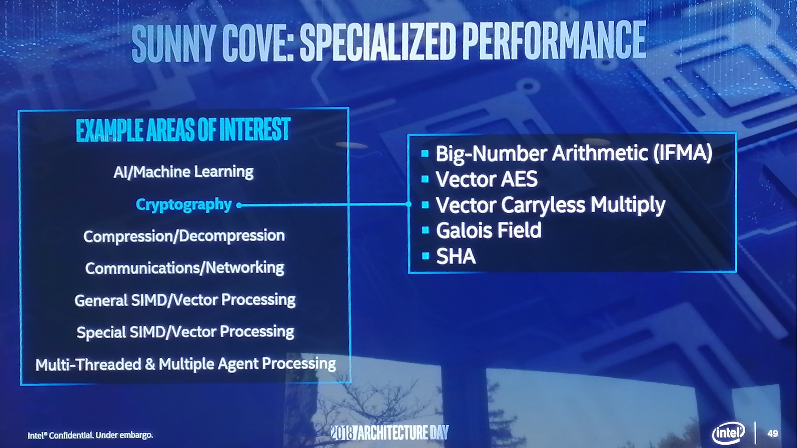
On top of the microarchitecture differences, there are new instructions for the Sunny Cove core to help speed up specialist compute tasks. With the AVX-512 unit in play, the new core will support IFMA instructions for big arithmetic compute, and which are also useful in cryptography. Along the same lines, Vector-AES (supporting more AES concurrently) and Vector Carryless Multiply are also supported. SHA and SHA-NI instructrions are also added, along with Galois Field instructions, which are fundamental building blocks in some elements of cryptography as well.
For Sunny Cove, there is also built-in support for larger memory capacities. The paging table for main memory is now a five layer design, up from four layers, supporting a Linear Address space up to 57 bits and a physical address space up to 52 bits. This means, according to Intel, that the server processors could theoretically support 4 TB of memory per socket. We will see Sunny Cove hit the market in the server space with Ice Lake-SP in 2020 according to Intel’s previous Xeon roadmaps. For security, Sunny Cove has access to Multi-Key Total Memory Encryption, and User Mode Instruction Prevention.
So where does this leave us in terms of Sunny Cove predicted performance compared to Skylake at a clock for clock level? Unfortunately we don’t have enough information. There is only enough to whet the appetite. Intel wants you (and me) to come back for more in 2019.


148 Comments
View All Comments
porcupineLTD - Thursday, December 13, 2018 - link
Can you articulate what you want to say with those links? or how they might contradict me/answer my question?ajc9988 - Thursday, December 13, 2018 - link
What I am saying with those links is that AMD has already evaluated the use of active interposers and is the company that is articulating a data protocol for active interposer routing so that it doesn't matter what each chiplet does on its own data routing, so that any chiplet could be attached to an active interposer and work. Further, in the 2017 white paper, it directly shows the reason that AMD hasn't yet adopted the active interposer is due to costs. Passive interposers can be used, but don't offer the benefit of active interposers. But, the cost of an active interposer is the same as doing a monolithic chip once the active interposer is produced on the 32nm or smaller active interposer. As such, adoption did not yet make sense until the costs are reduced.https://spectrum.ieee.org/tech-talk/semiconductors...
The earlier ones show AMD did research into the optimal topology for active interposers in 2014 and 2015. It shows the optimal core count for the benefit, latencies, etc.
Now, if you look at packaging solutions, say from GF, you find that 2.5D and 3D integration is only available on 32nm and 28nm processes, with 14nm coming soon. https://www.globalfoundries.com/sites/default/file...
I bring up GF doing the packaging as, due to the WSA, even if they cost more than competitors, being able to potentially count the wafers used for the active interposers against the WSA would reduce the fines payed under that contract for doing fabrication at TSMC, making it potentially, on net, cheaper.
Now, there is an article today from Anand saying Intel is releasing the B365 chipset on 22nm. ( https://www.anandtech.com/show/13714/intel-adds-b3... ) Intel was forced to move chipsets back to 22nm due to the 10nm process not being ready for mass deployment which caused a shortage of 14nm capacity. This means Intel could not shut down their 22nm fabs to cut that capacity. As such, a fab needs to stay as close to capacity as possible or else it bleeds money (hence why AMD eventually went fabless). So, Intel using 22nm fabs to do the 22nm active interposer is just Intel making lemonade on tech that few others adopted in the industry yet due to the basis of costs. If you go back to the cost study AMD did, the active interposer at 20nm is around the cost of doing a monolithic die, which is what Intel has done to date. So it isn't really costing them more to add in the active interposer at all, while saving expenditures by keeping the 22nm fabs full of jobs, while having awesome yields on the active interposers due to it being a very mature node with low defect rates, etc. If you examine the amount of area AMD estimated is needed for the logic routers, you can see only 1%-10% area on the active interposer is needed to achieve the goal, meaning the chances a critical defect hits the active interposer is very low.
But, as to it making AMD do it, that is the wrong thinking. AMD already plans to adopt it, just not until the costs of doing so are lower. They will check the IC Knowledge lists to see when costs make sense.
But, if you look at all that data I provided, AMD has all the solutions to the problems encountered with using an active interposer. All they are waiting for is it to be cost effective. Intel isn't leading anything here, other than doing it because they need to justify and subsidize having to keep certain 22nm fabs open because of their chipsets due to the delays in 10nm. Doesn't take a genius to figure it out, just takes someone paying attention to the tea leaves.
ajc9988 - Thursday, December 13, 2018 - link
Also, I forgot to mention that the 2.5D integration of HBM Phy onto a stitched interposer was accomplished last year. This suggests that HBM could be added to an active interposer when AMD eventually does adopt an active interposer. Meanwhile, with only 1-10% of the active interposer being used according to their papers, it leaves room for in the future having elements of the I/O chip being moved to the active interposer as an additional way that things easily could develop. The question is what benefit it would be to produce what on the 32nm or 28nm nodes over having their I/O disintegrated die on 14nm. But I would bet AMD has an idea of what would be better where and will consider it when eventually adopting, considered the detailed paper on routing topology of active interposers in that group of links.porcupineLTD - Thursday, December 13, 2018 - link
Thank you for the detailed response its very informative however its besides my comment, IF Intel ships its chiplet on interposer design in 2019 they will be first (regardless of the reasons or economics behind it), as for AMD not doing it now it's again besides my comment, I wandered if they will do this for ZEN 3 or 4 not ZEN2, ZEN 3 will launch in 2020 when (as far as I know) the WSA expires so what GF does or doesn't do is not that relevant (I would be curious to know about tsmc's or samsung's packaging/interposer offerings). The result (if they implement it in ZEN3/4) will come down to cost (as you point out), socket compatibility (can it be done on the current server socket?) and planning (ZEN3 design is almost done right now so even if the interposer cost is down AMD can't implement it if they didn't predict this one year ago).porcupineLTD - Thursday, December 13, 2018 - link
Also Anandtech, I am not versed in web design, but is it really that hard to have a comment section that doesn't utterly suck? Is it really that hard to introduce an edit function, or at least a delete one?(an upvote/donvote system would be asking for too much).ajc9988 - Thursday, December 13, 2018 - link
Forgive me, many think that Intel is showing through using it that they are significantly ahead in the field of active interposers and 2.5D and 3D chiplet integration, meaning that it would take years for other chip designers to catch up, which isn't the case. So I do apologize for that assumption in regards to you.What those do show is AMD does have plans to do so in the future, it is just a matter of timing. On the socket part, there is a chance they are introducing a new socket in order to support PCIe 4.0 on the upcoming Zen 2 chips, which comes from analyzing their wording from the Next Horizon event on Nov. 6th. Meanwhile, we know that PCIe 5.0 will be finalized potentially in the first half of next year and AMD did mention DDR5 potentially being available for Epyc 3 chips based on Zen 3, but that mainstream chips will not support DDR5 in 2020 (leaves open that TR HEDT platforms may or may not get DDR5 support at that time). Intel has not provided information on when PCIe 4.0, 5.0, or DDR5 will be supported. As such, though, AMD may have backwards compatibility on the CPUs for socket compatibility, but may require a new socket for the new boards containing the new features, which I think is understandable to many in the server and workstation spheres. It is also the reason I may wait for 2020 to upgrade my 1950X rather than next year (if you are going to buy a new board, and there is a chance that board won't contain the new feature sets that release that year, waiting one more year is fine IF your workloads won't suffer for the wait).
But, I read somewhere Intel hinted at 1GB of RAM being integrated with the active interposer processors, acting as an L4 cache. Although not novel (those articles I gave for AMD whitepapers from 2014 and 2015 specifically dealt with on package integration of memory and latencies involved, suggesting we could see some type of 3d memory solution integrated when AMD does incorporate an active interposer), seeing the latencies involved with Crystalwell, which was the eDRAM on Broadwell, suggests that Intel will get a significant uplift in certain workloads, as well as keeping the chip primed and having to go off chip less often for memory calls, which is fantastic. Intel also kept the power delivery part under wraps, which is something that does excite me, but we were given no information about it (possibly bringing FIVR back, which was rumored for Ice and Tiger lake anyways).
Also, on compatibility, part of the reason I gave the article discussing data protocols for active interposers is that the routing is chiplet agnostic, meaning you can integrate parts that have their own internal routing and not effect it. Then just comes down to appropriate socket wiring, which I mentioned they may need new sockets for these features, while just maintaining drop in compatibility for consumer side.
Here is some information on other packaging types out there in the market. I am including them, but as this is just being researched, I am not attesting veracity or relevance, fully. I will have glanced through them, but you understand.
http://s3.amazonaws.com/sdieee/1817-SanDiegoCPMTDL...
"DIGITIMES reports that the new TSMC plant in Chunan will be dedicated to offering the foundry’s in-house developed advanced packaging technologies: CoWoS (chip-on-wafer-on-substrate) and integrated fan-out (InFO) wafer-level packaging, and its newly-unveiled system-on-integrated-chips (SoIC) and wafer-on-wafer (WoW) packaging services."
https://criticalmaterials.org/tsmc-to-set-up-new-f...
https://fudzilla.com/news/pc-hardware/47265-tsmc-t...
https://electroiq.com/2018/10/synopsys-design-plat...
Older article for foundational work from 2014:
https://semiengineering.com/time-to-revisit-2-5d-a...
2016 follow up: https://semiengineering.com/2-5d-becomes-real/
Packaging Market from February 2018:
http://worldherald24.com/2018/02/19/global-3d-ic-a...
Paper and slide show discussing the implementation and challenges of 3D packaging from 2016:
https://smtnet.com/library/files/upload/25d-3d-sem...
Sorry for the data dump at the end. I do apologize about that.
tommybobberson - Saturday, December 15, 2018 - link
just clarifying, do you mean to use such methods, amd would need to rive up production costs which reduces their profit/value. but since intel already has a high production cost, such methods would not affect them?ajc9988 - Wednesday, December 19, 2018 - link
tommybobberson - in a manner of speaking, yes. How much it costs to produce effects margins and pricing. One reason AMD could price the high core chips in such a manner, aside from effective yields for products, is the decreased costs to produce high core count products. If AMD added the active interposer now, it would rise production costs to be the same as a monolithic die, which would then require either an increase in market price of the products or a decrease in margins for their products.Intel, on the other hand, never captured the extra margin of going to chiplets before introducing the stacked chips. That means that the active interposer cost to them is less as the price to do so matches the cost of a monolithic die. As such, Intel can maintain their current pricing while introducing the stacked die on active interposer. Further, due to filling up 22nm fab time (because of 10nm causing a shortage of 14nm fab time which required Intel to move certain lines back to 22nm, likely forcing some plants planned to be closed or retrofitted to remain on 22nm), Intel will be able to help on the cost of 10nm delay, thereby mitigating some of the effects found in not having 10nm up and running by now.
Supercell99 - Friday, December 14, 2018 - link
With all the hackers, PC gaming is dying.sgeocla - Wednesday, December 12, 2018 - link
Fist they mock your chiplets by saying you glue your dies together, then they fail to compete with you and then years after they copy your chiplets and call it revolutionary.This is why Intel can no longer have public presentations of their own failures and have to have privately controlled presentations.