The NVIDIA GeForce GTX 1080 Preview: A Look at What's to Come
by Ryan Smith on May 17, 2016 9:00 AM EST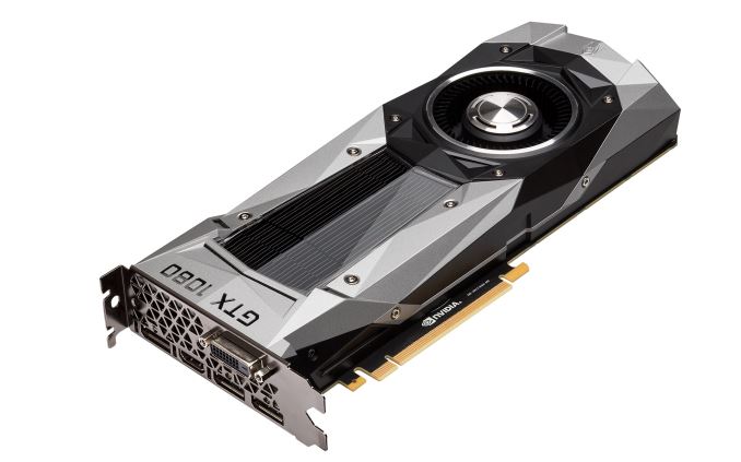
Earlier this month NVIDIA announced their latest generation flagship GeForce card, the GeForce GTX 1080. Based on their new Pascal architecture and built on TSMC’s 16nm FinFET process, the GTX 1080 is being launched as the first 16nm/14nm-based video card, and in time-honored fashion NVIDIA is starting at the high-end. The end result is that the GTX 1080 will be setting the new high mark for single-GPU performance.
Unlike past launches, NVIDIA is stretching out the launch of the GTX 1080 a bit more. After previously announcing it back on May 6th, the company is lifting their performance and architecture embargo today. Gamers however won’t be able to get their hands on the card until the 27th – next Friday – with pre-order sales starting this Friday. It is virtually guaranteed that the first batch of cards will sell out, but potential buyers will have a few days to mull over the data and decide if they want to throw down $699 for one of the first Founders Edition cards.
As for the AnandTech review, as I’ve only had a few days to work on the article, I’m going to hold it back rather than rush it out as a less thorough article. In the meantime however, as I know everyone is eager to see our take on performance, I wanted to take a quick look at the card and the numbers as a preview of what’s to come. Furthermore the entire performance dataset has been made available in the new GPU 2016 section of AnandTech Bench, for anyone who wants to see results at additional resolutions and settings.
Architecture
| NVIDIA GPU Specification Comparison | ||||||
| GTX 1080 | GTX 980 Ti | GTX 980 | GTX 780 | |||
| CUDA Cores | 2560 | 2816 | 2048 | 2304 | ||
| Texture Units | 160 | 176 | 128 | 192 | ||
| ROPs | 64 | 96 | 64 | 48 | ||
| Core Clock | 1607MHz | 1000MHz | 1126MHz | 863MHz | ||
| Boost Clock | 1733MHz | 1075MHz | 1216MHz | 900Mhz | ||
| TFLOPs (FMA) | 9 TFLOPs | 6 TFLOPs | 5 TFLOPs | 4.1 TFLOPs | ||
| Memory Clock | 10Gbps GDDR5X | 7Gbps GDDR5 | 7Gbps GDDR5 | 6Gbps GDDR5 | ||
| Memory Bus Width | 256-bit | 384-bit | 256-bit | 384-bit | ||
| VRAM | 8GB | 6GB | 4GB | 3GB | ||
| FP64 | 1/32 | 1/32 | 1/32 FP32 | 1/24 FP32 | ||
| TDP | 180W | 250W | 165W | 250W | ||
| GPU | GP104 | GM200 | GM204 | GK110 | ||
| Transistor Count | 7.2B | 8B | 5.2B | 7.1B | ||
| Manufacturing Process | TSMC 16nm | TSMC 28nm | TSMC 28nm | TSMC 28nm | ||
| Launch Date | 05/27/2016 | 06/01/2015 | 09/18/2014 | 05/23/2013 | ||
| Launch Price | MSRP: $599 Founders $699 |
$649 | $549 | $649 | ||
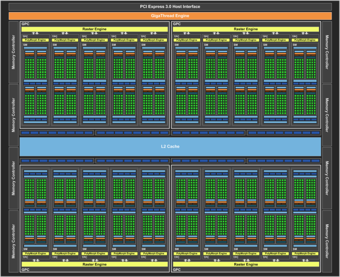
While I’ll get into architecture in much greater detail in the full article, at a high level the Pascal architecture (as implemented in GP104) is a mix of old and new; it’s not a revolution, but it’s an important refinement. Maxwell as an architecture was very successful for NVIDIA both at the consumer level and the professional level, and for the consumer iterations of Pascal, NVIDIA has not made any radical changes. The basic throughput of the architecture has not changed – the ALUs, texture units, ROPs, and caches all perform similar to how they did in GM2xx.
Consequently the performance aspects of consumer Pascal – we’ll ignore GP100 for the moment – are pretty easy to understand. NVIDIA’s focus on this generation has been on pouring on the clockspeed to push total compute throughput to 9 TFLOPs, and updating their memory subsystem to feed the beast that is GP104.
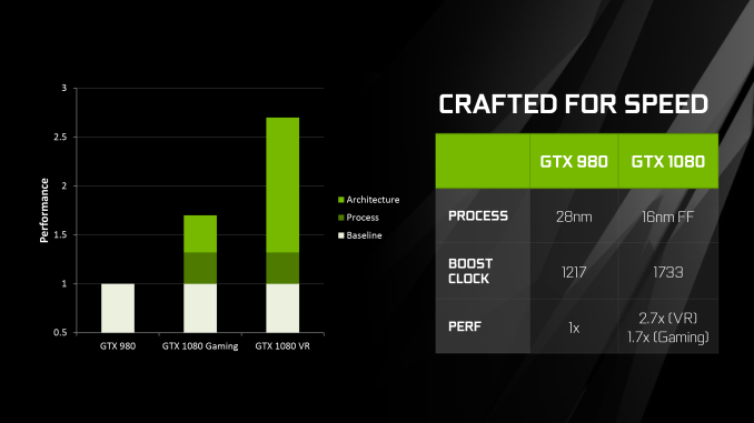
On the clockspeed front, a great deal of the gains come from the move to 16nm FinFET. The smaller process allows NVIDIA to design a 7.2B transistor chip at just 314mm2, while the use of FinFET transistors, though ultimately outright necessary for a process this small to avoid debilitating leakage, has a significant benefit to power consumption and the clockspeeds NVIDIA can get away with at practical levels of power consumption. To that end NVIDIA has sort of run with the idea of boosting clockspeeds, and relative to Maxwell they have done additional work at the chip design level to allow for higher clockspeeds at the necessary critical paths. All of this is coupled with energy efficiency optimizations at both the process and architectural level, in order to allow NVIDIA to hit these clockspeeds without blowing GTX 1080’s power budget.
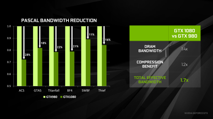
Meanwhile to feed GTX 1080, NVIDIA has made a pair of important changes to improve their effective memory bandwidth. The first of these is the inclusion of faster GDDR5X memory, which as implemented on GTX 1080 is capable of reaching 10Gb/sec/pin, a significant 43% jump in theoretical bandwidth over the 7Gb/sec/pin speeds offered by traditional GDDR5 on last-generation Maxwell products. Coupled with this is the latest iteration of NVIDIA’s delta color compression technology – now on its fourth generation – which sees NVIDIA once again expanding their pattern library to better compress frame buffers and render targets. NVIDIA’s figures put the effective memory bandwidth gain at 20%, or a roughly 17% reduction in memory bandwidth used thanks to the newer compression methods.
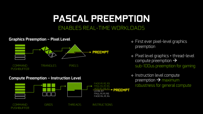
As for features included, we’ll touch upon that in a lot more detail in the full review. But while Pascal is not a massive overhaul of NVIDIA’s architecture, it’s not without its own feature additions. Pascal gains the ability to pre-empt graphics operations at the pixel (thread) level and compute operations at the instruction level, allowing for much faster context switching. And on the graphics side of matters, the architecture introduces a new geometry projection ability – Simultaneous Multi-Projection – and as a more minor update, gets bumped up to Conservative Rasterization Tier 2.
Looking at the raw specifications then, GTX 1080 does not disappoint. Though we’re looking at fewer CUDA cores than the GM200 based GTX 980 Ti or Titan, NVIDIA’s significant focus on clockspeed means that GP104’s 2560 CUDA cores are far more performant than a simple core count would suggest. The base clockspeed of 1607MHz is some 42% higher than GTX 980 (and 60% higher than GTX 980 Ti), and the 1733MHz boost clockspeed is a similar gain. On paper, GTX 1080 is set to offer 78% better performance than GTX 980, and 47% better performance than GTX 980 Ti. The real world gains are, of course, not quite this great, but they’re also relatively close to these numbers at times.




262 Comments
View All Comments
Ushio01 - Tuesday, May 17, 2016 - link
Could this be more underwhelming? guess I can skip this gen and keep my 670 for another few years.Jtaylor1986 - Tuesday, May 17, 2016 - link
This card exists in the zone of being overpowered at 1080P and 1440P and still a hair too slow at 4k in some titles. I guess we will have to wait until the big die 14/16nm gpus come out before we get no compromise 4k.FMinus - Tuesday, May 17, 2016 - link
If you have a 980Ti, overclock it (it probably already is) and it's going hand to hand with the stock 1080, no need to upgrade really.Looking at the reviews right now, I doubt the 1070 will even touch the 980Ti, and if they keep the EU pricing up, highly overpriced at 460-520EUR, for what it delivers. So I'm just gonna wait for what AMD brings to the table.
TheinsanegamerN - Tuesday, May 17, 2016 - link
Or wait for 3rd party models. Techspot showed pretty good gains from OCing, so the big coolers(or liquid cooling) that can hit 2+GHz are going to be where the 1080 shines.jasonelmore - Tuesday, May 17, 2016 - link
EU pricing is high because of VAT not currency exchange.BrokenCrayons - Tuesday, May 17, 2016 - link
If you're not trying to drive 4k resolutions, there probably isn't a compelling reason to upgrade from a 670 until the generation after the 10x0. I do agree that the 1080 strikes me as "yet another GPU refresh" because the performance increase isn't significant and the power/thermal numbers are only holding steady despite the more efficient FinFET process.I'm still interested in reading the full review, but at this point Ryan's comment about AMD's possible future plans - "Rather the company is looking to make a run at the much larger mainstream market for desktops and laptops with their Polaris architecture, something that GP104 isn’t meant to address." is far more interesting to me since I'd like to see the new process node put to use in laptops and in lower end portions of the GPU market.
DanNeely - Tuesday, May 17, 2016 - link
The GP106 (presumably 1060/1050) is due out in the fall.AMD will initially have the middle of the market to itself. It'll be interesting to see how well they're able to exploit it though. Not having a true flagship until Vega launches will hurt them among the large body of ignorant consumers who look at the headline numbers for top of the line cards because they're the most visible and buy based on that; a problem that's been dogging them for the last few years as nVidia has grown its market share.
The biggest question is if the lack of a flagship at launch is due to due to the unavailability of HBM (ie Vega doesn't have GDDR5/x memory controllers at all) or a deliberate decision to go for the center of the market first; or is an indicator that GloFo is struggling on 14nm yields. The latter is alarming if true; since it would mean that despite probably being able to crush nVidia in the mid-range for the next few months limited availability would prevent them from being able to exploit their lead effectively at a time when AMD desperately needs a cash cow generating win somewhere.
medi03 - Tuesday, May 17, 2016 - link
PS4k is to be released in October this year (major French retailer leak) so 14nm should be there.Also, remember that it's actually Samsung's 14nm.
BrokenCrayons - Tuesday, May 17, 2016 - link
Yes, there's no question that there'll be some lost sales over the impression of market leadership that spills over into unrelated segments where that competition for the fastest high end GPU isn't really relevant. Buyers who don't look at the value proposition of the specific product they're purchasing relative to its price bracket are pretty commonplace when it comes to computer components. I think it might hurt AMD's bottom line, but maybe not if the mid range volume is high enough to offset those lost sales.With respect to 14nm yields, I'd think that positioning the company to tackle the middle of the GPU price/performance market would be exceptionally unwise if there were problems with yield so I'd don't think it's worth worrying much about. Lower end GPUs use less wafer and that might offer an advantage, but lower priced cards sell in larger numbers typically than the top end cards so the demand will be higher and expectations for fab output might be higher as well. I'd like to think the decision is deliberate. AMD has also exhibited a history of targeting unfilled or less well served segments in order to find a niche that generates sales when they aren't in a position to lead in performance as demonstrated by their dropping out of the high end CPU market. That might be a bad strategy though since it hasn't done them any favors at retaining CPU market share and it does look like they're following a similar course with graphics.
I'm not sure what to think really, but I will be keeping an eye out for AMD's upcoming graphics products as they're released since they may offer more value for the dollar. I don't really need a lot of GPU since I keep resolutions low and use Steam's streaming exclusively now, but I would like to upgrade out of the GT 730 with a 16/14nm card that offers a little more of everything, but stays in a reasonable power budget.
Lolimaster - Tuesday, May 17, 2016 - link
Considering that the gpu in the current gen A10 APU's destroys your GT730. the 50w Polaris 11 will probably deliver around GTX960/370 performance.