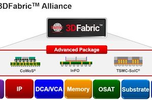
3DFabric
This year TSMC is commemorating 15 years of its Open Innovation Platform, a multi-faceted program that brings together the foundry's suppliers, partners, and customers to help TSMC's customers better build innovative chips in an efficient and timely manner. The OIP program has grown over the years and now involves tens of companies and over 70,000 IP solutions for a variety of applications. It continues to grow, and its importance will get higher than ever when next generation technologies, such as 2 nm, and advanced packaging methods become mainstream in the coming years. "This is not a marketing program, it is actually an engineering program to enable the industry," said Dan Kochpatcharin, Head of Design Infrastructure Management at TSMC, at the OIP 2023 conference in Amsterdam...
TSMC Opens Advanced Backend Packaging Fab for AI and HPC Products
TSMC on Friday formally opened its Advanced Backend Fab 6 facility, which it will be using to expand the company's capacity for building high-end, multi-chiplet products. The facility is...
1 by Anton Shilov on 6/9/2023
As HPC Chip Sizes Grow, So Does the Need For 1kW+ Chip Cooling
One trend in the high performance computing (HPC) space that is becoming increasingly clear is that power consumption per chip and per rack unit is not going to stop...
40 by Anton Shilov on 6/27/2022
An AnandTech Interview with TSMC: Dr. Kevin Zhang and Dr. Maria Marced
In the past week, TSMC ran its 2021 Technology Symposium, covering its latest developments in process node technology designed to improve the performance, costs, and capabilities for its customers...
18 by Dr. Ian Cutress on 6/8/2021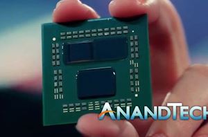
AMD Demonstrates Stacked 3D V-Cache Technology: 192 MB at 2 TB/sec
The AMD team surprised us here. What seemed like a very par-for-the-course Computex keynote turned into an incredible demonstration of what AMD is testing in the lab with TSMC’s...
93 by Dr. Ian Cutress on 5/31/2021
3DFabric: The Home for TSMC’s 2.5D and 3D Stacking Roadmap
Interposers. EMIB. Foveros. Die-to-die stacking. ODI. AIB.TSVs. All these words and acronyms have one overriding feature – they are all involved in how two bits of silicon physically connect...
9 by Dr. Ian Cutress on 9/2/2020
TSMC’s Version of EMIB is ‘LSI’: Currently in Pre-Qualification
Whilst process node technologies and Moore’s Law are slowing down, manufacturers and chip designers are looking to new creative solutions to further enable device and performance scaling. Advanced packaging...
19 by Andrei Frumusanu on 8/25/2020


