The NVIDIA GeForce GTX 1080 Ti Founder's Edition Review: Bigger Pascal for Better Performance
by Ryan Smith on March 9, 2017 9:00 AM ESTMeet the GeForce GTX 1080 Ti Founder’s Edition
When it comes to the design of the GeForce GTX 1080 Ti Founder’s Edition, if you’ve seen a high-end NVIDIA card in the last 4 years then you know roughly what to expect. NVIDIA has found their sweet spot in card design, and while the GTX 1080 Ti does have a few wrinkles of its own, it’s not a radical departure from the likes of the GTX 1080, GTX 980 Ti, or GTX 780 Ti. GeForce GTX 1080 Ti is a traditional NVIDIA reference card, with all the competence, performance, and functionality that entails.
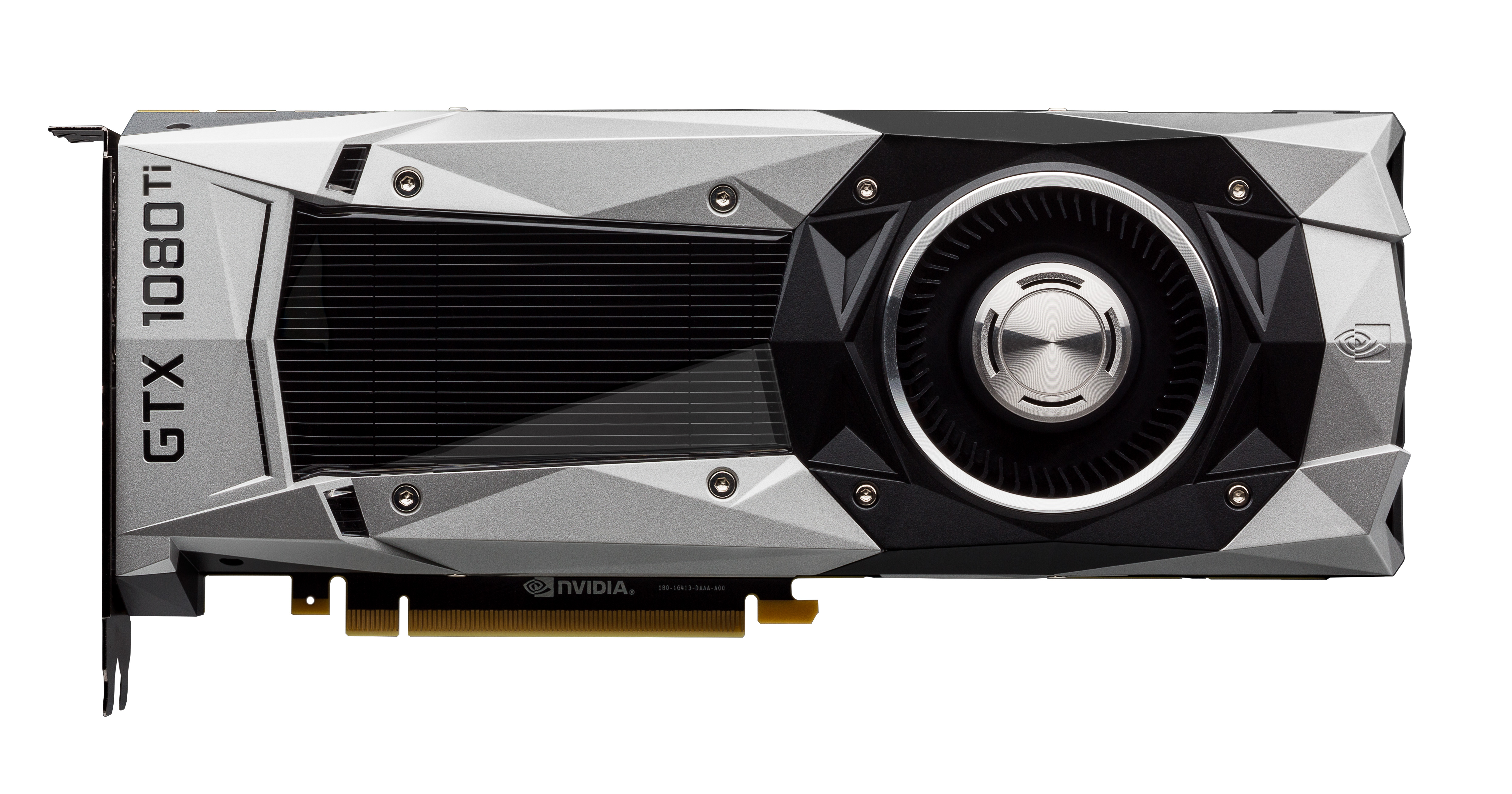
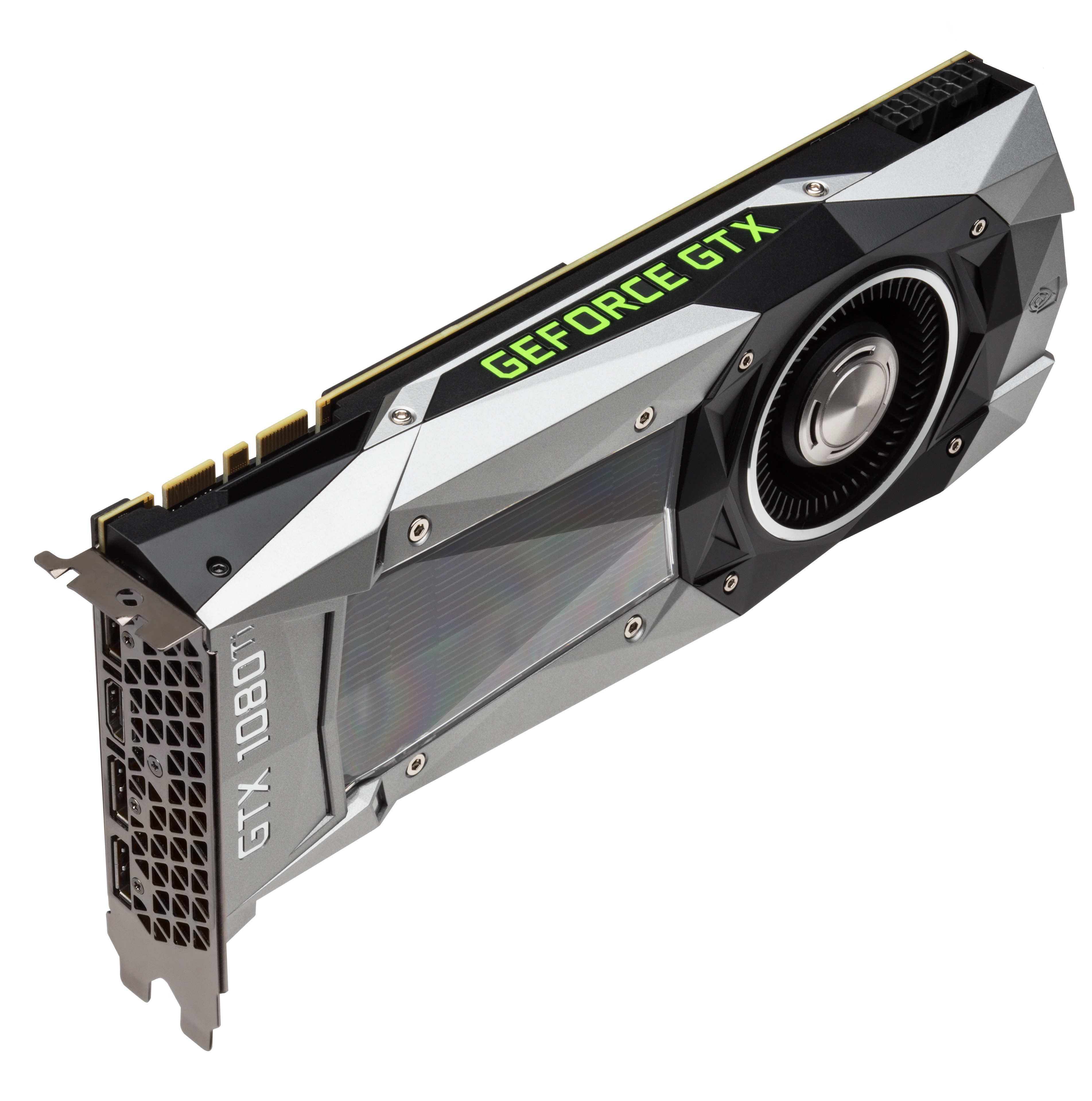
At a high level, the GTX 1080 Ti Founder’s Edition is a 10.5-inch long blower-type card comprised of a cast aluminum housing and held together using a combination of rivets and screws. Designed as much for aesthetics as functionality, NVIDIA’s use of well-secured metal has done a good job of tempering noise generation, and for those who like to show off their rigs, the basic design and LED-backlit logo are unmistakable.
Cracking open the card and removing the shroud exposes the card’s fan and heatsink assembly. Once again NVIDIA is lining the entire card with an aluminum baseplate, which provides heatsinking capabilities for the VRMs and other discrete components below it, along with providing additional protection for the board. Like past NVIDIA 250W cards, the GTX 1080 FE uses NVIDIA’s vapor chamber cooler in order to maximize the heat transfer between the GPU/VRMs/DRAM and the aluminum heatsink above. As far as blower-type cards go, it’s still the card to beat.
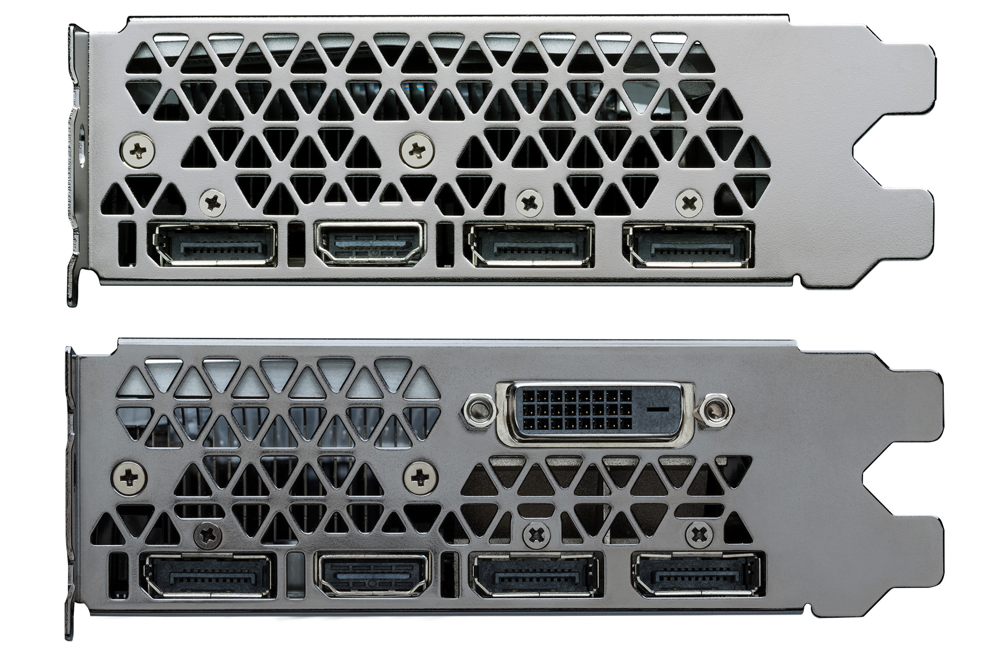
Airflow: GTX 1080 Ti vs. GTX 1080
For the GTX 1080 Ti, NVIDIA has refined this basic design just a bit in order to further increase airflow. The key change here is that NVIDIA has removed the DVI port that in past designs took up part of the second slot used for ventilation. Consequently the entire slot is now open for airflow. As we’ll see in our benchmarks the practical difference in noise is not very much, but it still means the GTX 1080 Ti is quieter than the GTX 980 Ti and GTX 780 Ti that came before it.
Otherwise in a blink-and-you’ll-miss-it kind of change, NVIDIA has also tweaked the tapering of the shroud itself to maximize the airflow. It’s difficult to pick up in pictures, but the shroud is just a bit thinner and the bottom of the shroud is just a bit higher, allowing just a bit more unobstructed airflow through the card. This subtle change is a good example of where NVIDIA is in their card design cycle: with the major performance elements of the cooler design essentially being a solved problem, NVIDIA is now toying with small changes to eke out just a bit more performance.
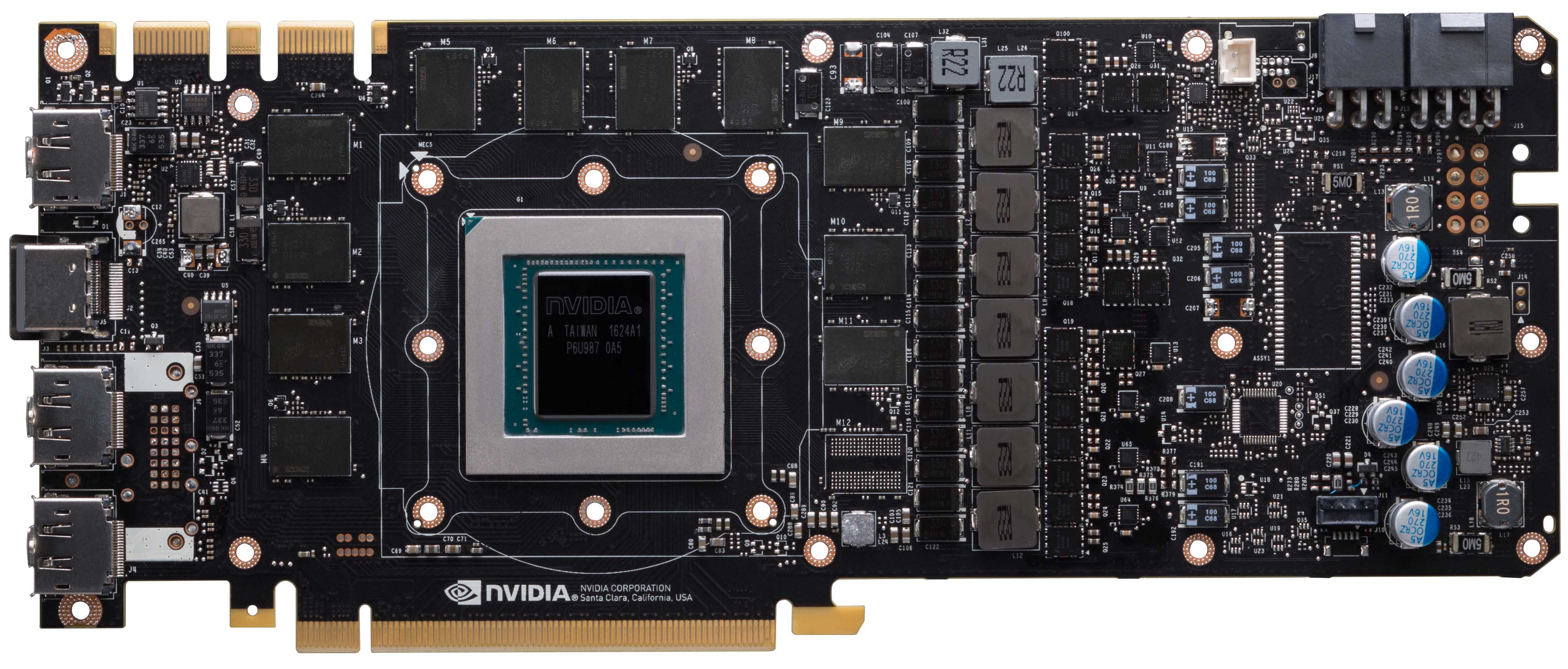
Popping off the cooler, we see NVIDIA’s reference PCB. This appears to be the same PCB used on the similarly configured GP102-based Titan X Pascal, and is consistent with NVIDIA’s past reuse of PCBs.
Of particular note, we can see that NVIDIA has equipped the card with a surprising number of MOSFETs, and it turns out there’s a good reason for this. For the GTX 1080 Ti, NVIDIA has opted to go with two dualFETs for each of the GPU’s 7 power phases, as opposed to the traditional 1-per-phase design used in most NVIDIA cards. While this drives up the total cost of the card a bit, the payoff is that it improves on the card’s power delivery efficiency a bit, especially at the 200W+ range the GTX 1080 Ti operates in.
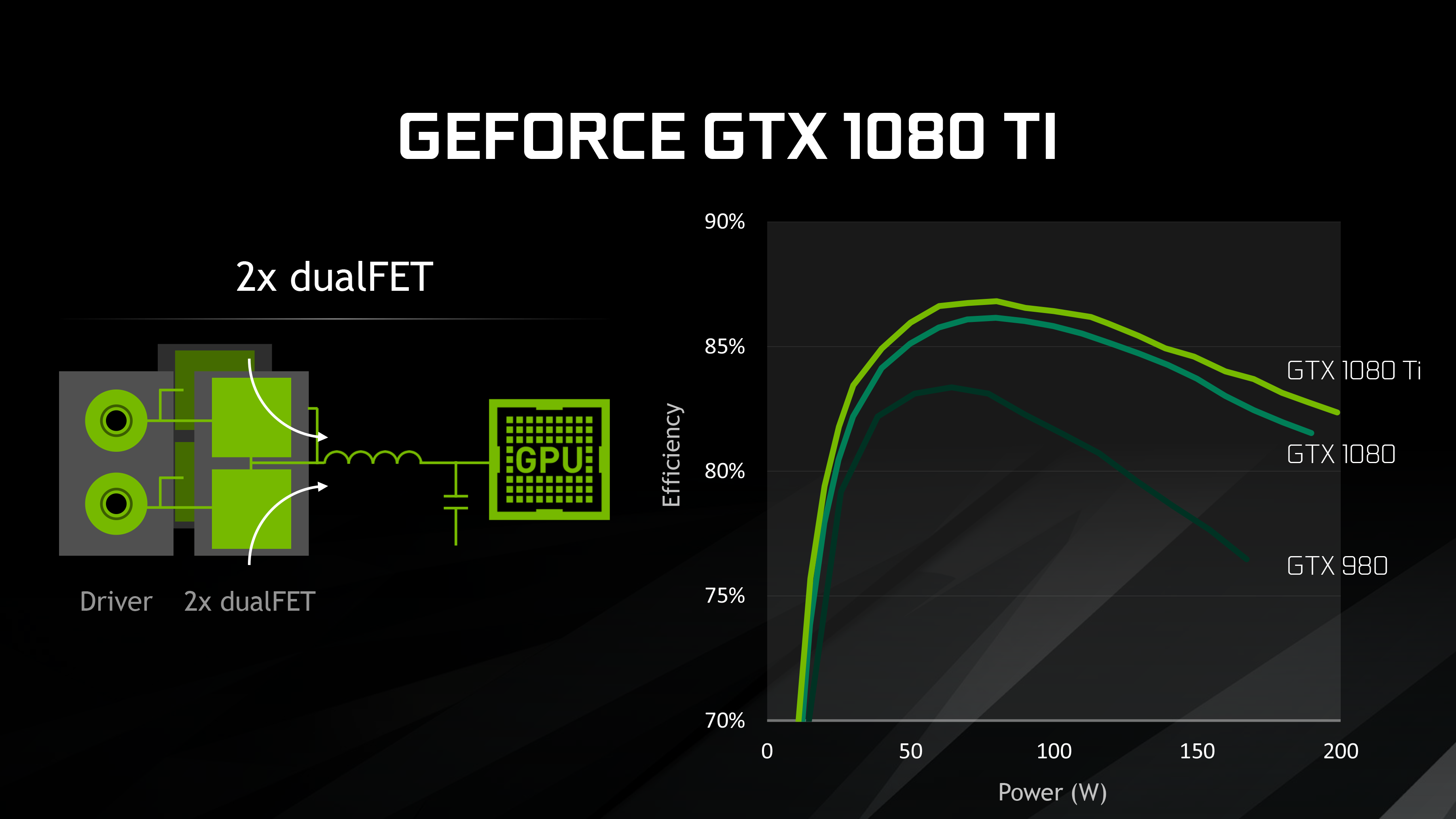
This isn’t the first overall GeForce card we’ve seen with a large number of MOSFETs – NVIDIA’s board partners at times treat it as a contest in and of itself – but this is the first time we’ve seen NVIDIA use such a large number and promote it. Generally speaking additional phases and MOSFETs can improve a power delivery subsystem by spreading out the load – and in a game of inches, every bit counts – but the additional MOSFETs are subject to diminishing returns both at idle and load.
Otherwise this is a fairly typical NVIDIA PCB. The reuse of the Titan PCB means that the board should work with water blocks and other add-ons designed for the Titan, though I suspect for best overclocking results the hardcore overclockers will continue to want to look to more specialized designs from the likes of MSI, EVGA, Asus, and others.
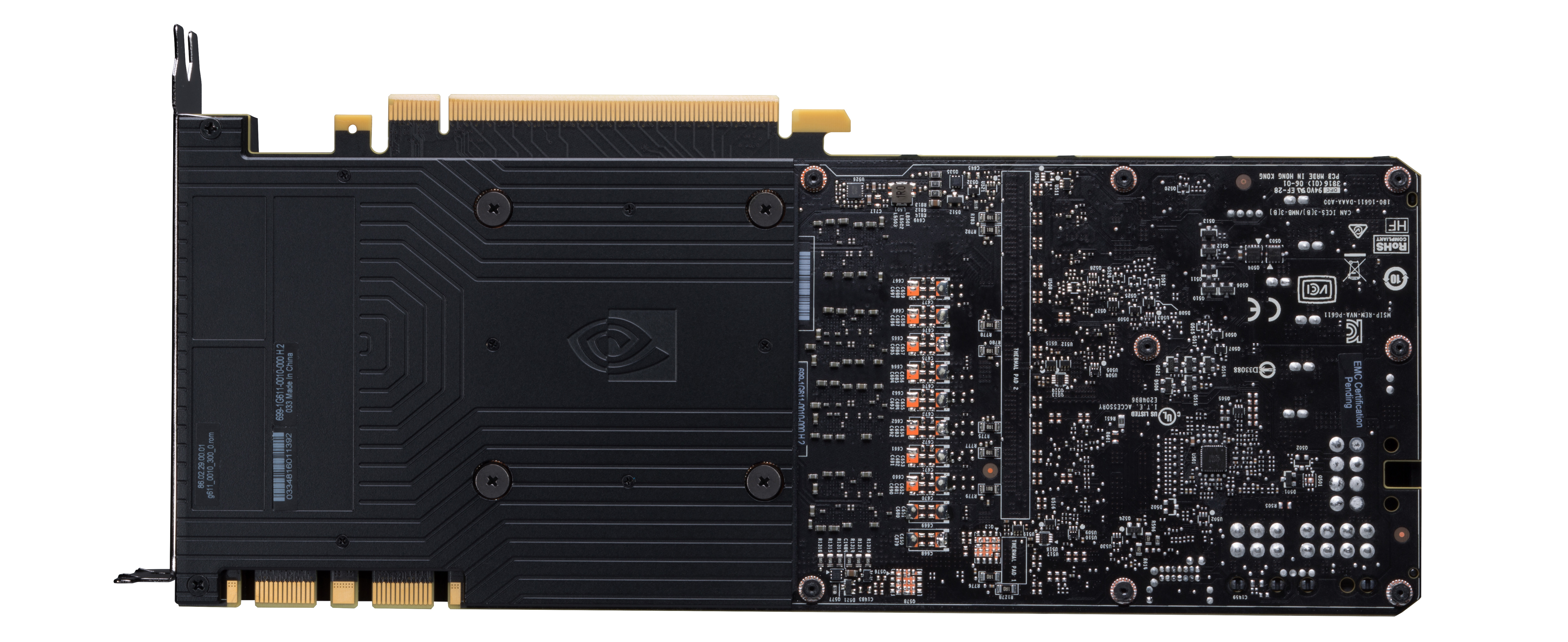
Flipping the card over to the back, we find NVIDIA’s now-standard segmented backplate. The presence of the backplate helps to protect the card, but one or both segments can be removed to add precious millimeters of room for airflow in tightly packed SLI designs.
Moving on, towards the top of the card we find the requisite SLI and power connectors. Like NVIDIA’s 250W cards before it, the GTX 1080 Ti features a 6 pin + 8 pin setup. NVIDIA’s 250W limit means that, on-board circuitry aside, the power delivery system isn’t anywhere close to its 300W limit. Otherwise we find a pair of SLI connectors, which like the rest of the GTX 10-series cards are designed for use with NVIDIA’s latest-generation High Bandwidth (HB) bridges.
Finally, getting back to NVIDIA’s display I/O configuration, as we mentioned earlier NVIDIA has removed the DVI port from the card in favor of giving the card unobstructed airflow for better cooling. As a result, the card features only modern ports: 3x DisplayPort 1.4 and 1x HDMI 2.0b. With that said, as a consolation item of sorts for the remaining DVI users, NVIDIA is including a DisplayPort-to-SL-DVI adapter with the Founder’s Edition card. This doesn’t perfectly replace the missing DVI port – in particular, it can’t drive 2560x1440 or 2560x1600 displays – but for lower resolution displays it will do the trick. But if it’s not already clear from this change and the number of motherboards to drop DVI over the years, DVI’s days are numbered, and we’re only going to continue to see DVI ports go away at this point.


161 Comments
View All Comments
Jon Tseng - Thursday, March 9, 2017 - link
Launch day Anandtech review?My my wonders never cease! :-)
Ryan Smith - Thursday, March 9, 2017 - link
For my next trick, watch me pull a rabbit out of my hat.blanarahul - Thursday, March 9, 2017 - link
Ooh.YukaKun - Thursday, March 9, 2017 - link
/clapsGood article as usual.
Cheers!
Yaldabaoth - Thursday, March 9, 2017 - link
Rocky: "Again?"Ryan Smith - Thursday, March 9, 2017 - link
No doubt about it. I gotta get another hat.Anonymous Blowhard - Thursday, March 9, 2017 - link
And now here's something we hope you'll really like.close - Friday, March 10, 2017 - link
Quick question: shouldn't the memory clock in the table on the fist page be expressed in Hz instead of bps being a clock and all? Or you could go with throughput but that would be just shy of 500GBps I think...Ryan Smith - Friday, March 10, 2017 - link
Good question. Because of the various clocks within GDDR5(X)*, memory manufacturers prefer that we list the speed as bandwidth per pin instead of frequency. The end result is that the unit is in bps rather than Hz.* http://images.anandtech.com/doci/10325/GDDR5X_Cloc...
close - Friday, March 10, 2017 - link
Probably due to the QDR part that's not obvious from reading a just the frequency. Thanks.