
Original Link: https://www.anandtech.com/show/396
VIA Apollo Pro 133A & VCSDRAM - Part 1: The Technology
by Anand Lal Shimpi on October 18, 1999 11:28 PM EST- Posted in
- CPUs
Just two months ago we took a look at VIA's latest Slot-1 chipset, the VIA Apollo Pro 133, which boasted the title of being the first Slot-1/Socket-370 chipset with official support for the 133MHz FSB. Unfortunately, the design was based upon somewhat outdated technology because it did not support AGP 4X, something Intel was scheduled to announce support for within the following two months with the i820 chipset.
Two months passed and Intel never made the announcement for the i820 chipset. The cause for this 'delay of game' ended up being the layout of i820 motherboards that featured 3 RDRAM slots, not the modules and not the chipset itself. The problem seems quite minor but it kept Intel from taking the spotlight in September for releasing the next flagship chipset platform for desktop PCs. This paved the way for VIA to quietly introduce the successor to their 133MHz-chipset platform just two months after they made the move to 133MHz.
This new chipset isn’t really new at all; instead, it is a somewhat modified version of the North Bridge we've seen in VIA's Apollo Pro 133 thus justifying the small change in the name of this chipset solution. The part has been dubbed the Apollo Pro 133A and is essentially identical to the Apollo Pro 133 in every aspect except it adds the support for AGP 4X, making it a true competitor to Intel's 820. Why even bother with anything other than the i820? Intel has always produced high quality and high performing chipsets in the past, why even consider VIA?
There are a number of reasons for straying from Intel's solutions, especially the i820. With the i440BX the decision was easy to make; VIA's solution did not perform as well as the BX and it offered no features that the BX didn't. The BX was widely used and accepted and when you finally had it, you didn't need to manually install any special drivers to make the BX platform perform like it should. While the latter is a fault of the Operating System, in general, the VIA Apollo Pro+ (VIA's BX competitor) offered no real advantages over the Intel BX so most disregarded it.
The i820 isn't simply a BX chipset with the addition of support for the 133MHz FSB, AGP 4X, and Ultra ATA 66. If it was, then the decision would be simple since the BX is already a proven chipset. Instead, the i820, as we know from our review of the chipset, strays from the memory standard that we've been used to since before the release of the LX chipset in 1997 and moves towards Rambus DRAM. The main problem the industry as a whole has with Rambus or RDRAM is that the technology is expensive to implement and the performance gains are minimal for most users. The technology itself is perfectly sound, it offers a high bandwidth solution thus catering to Intel's recent philosophy that memory bandwidth is an obvious bottleneck of our PCs. But since today's performance numbers indicate that very little improvement is provided by i820 systems with the high speed RDRAM, the added cost isn't worth it. So, what other options are there?
If the Apollo Pro+ was designed to be a direct competitor to the BX chipset, then the new Apollo Pro 133A is essentially a competitor to the BX that adds support for the 133MHz FSB, AGP 4X and Ultra ATA 66. Sound familiar? Definitely, it's what we just talked about as being what many wanted the i820 to be.
The North Bridge
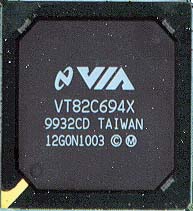 Feature-wise, the Apollo Pro 133A is
just what the doctor ordered, it combines all of the "next-generation" features
that we're looking for. Although it may not offer the same amount of memory bandwidth as
the i820, it is definitely a good solution for current 133MHz FSB CPUs, at least until
RDRAM takes off as the next standard as Intel is claiming it will become.
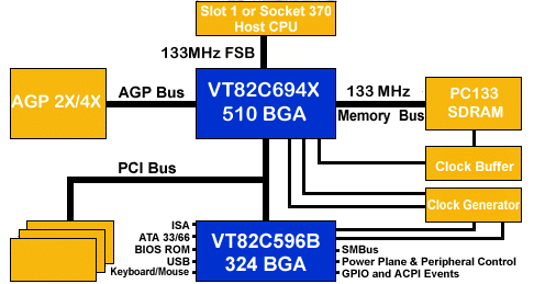
The chipset, like all of VIA's solutions, uses the familiar North/South Bridge construction with the memory, AGP and CPU interactions controlled by the North Bridge and all other peripherals (i.e. IDE controllers, PCI bus, etc…) controlled by the South Bridge. How does the new North Bridge make the Apollo Pro 133A what it is?
The North Bridge that makes up the chipset is the VIA VT82C694X as is seen to the right. This is the first VIA North Bridge to be manufactured out of National Semiconductor's fabrication plants, which VIA acquired earlier this year, hence the National Semiconductor logo.
The 694X is virtually identical to VIA's VT82C693A that was present as the North Bridge on Apollo Pro 133 boards. It supports the 1/2 AGP clock divider, the 133MHz FSB frequency as well as asynchronous operation of the memory bus at either the FSB frequency, FSB - 33MHz or FSB + 33MHz (combinations greater than 133MHz are not supported). This means that the memory frequencies supported by the chipset are 66MHz, 100MHz, and 133MHz. It also allows you to combine a 133MHz FSB CPU with slower PC100 SDRAM that doesn't cut it at 133MHz.
In terms of memory support, both the 694X and the older 693A support SDRAM, HSDRAM and Virtual Channel SDRAM. The read/write buffers and memory timings remain unchanged from the 693A so performance should be identical to that of the Apollo Pro 133A.
The only real difference is the addition of AGP 4X support to the chipset. This addition unfortunately increases the pin count of the 694X from 492 pins to 510 pins, making the new North Bridge incompatible with older designs. The downside to this is that it means that a motherboard manufacturer can't just 'pop' in the new North Bridge into their older 693A designs; they have to actually provide a small amount of redesigning. Fortunately the cost of adjusting a 693A design to the new 694X North Bridge is not that great, but it is a reason why you haven't seen many motherboards based on the 694X. At this year's Fall Comdex in Las Vegas we'll definitely see a number of Slot-1 and Socket-370 solutions built on the new 694X, the support for the platform is definitely there.
The CPU support that the 694X brings to the table is identical to what the BX, i820, and the older 693A offer. The chipset supports all Slot-1 CPUs including the forthcoming Pentium III E (aka Coppermine); just make sure that the particular motherboard you're interested in supports the 1.65v core voltage of the Pentium III E and you'll be fine.
As with all other VIA North Bridges, the 694X requires VIA's own GART drivers to enable full AGP 2X/4X transfer rates. This driver is available at VIA's page and has no incompatibilities with the current crop of graphics accelerators on the market, including NVIDIA's GeForce 256. VIA has come a long way since their original AGP chipsets were released for the Socket-7/Super7 platform; they have improved on the once horrendous compatibility problems their chipsets were plagued with.
The South Bridge
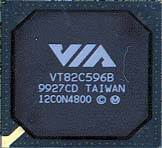 The official South Bridge
counterpart to the 694X is the VT82C596B Mobile South Bridge. The 596B is a part
we've already known for quite some time. It is an evolved version of the 596 South Bridge
that adds support for Ultra ATA 66 which is denoted by the addition of the 'B' to the
title.
The 596B has been in production for quite some time and is already implemented in many motherboard designs. The chip is pin compatible with the 324-pin 686A Super South Bridge. The difference between the 596B and the 686A is that the 686A includes integrated Hardware Monitoring and support for an AMR slot and, consequently, Audio/Telephony (Modem) codecs. Motherboard manufacturers will be allowed to pick and choose from the 596B or the 686A for their Apollo Pro 133A solutions but, most likely, you’ll see the 596B in most boards until the demand for AMR rises.
The combination of the 694X North Bridge and the 596B South Bridge make for a platform that is, feature-wise, everything the BX was, while adding support for the 133MHz FSB, AGP 4X and Ultra ATA 66.
What about overclocking?
Although most BX motherboards already support FSB frequencies of 133MHz and above, the problem with overclocking the FSB past 100MHz on current BX and Apollo Pro Plus motherboards is the frequency it places the rest of your system at. The problem with the North/South bridge architecture of most of our chipsets is that most of the operating frequencies are dependent upon one another. For example, if you overclock your FSB to 133MHz (on a 100MHz BX board) your PCI bus that was once running at 100MHz/3 is now running at 133MHz/3. Granted that most newer boards now support the 1/4 PCI clock divider which would put your PCI bus at 133MHz/4, but what about your AGP card?
The current AGP 2X/4X specification calls for a 66MHz clock frequency of all AGP cards (AGP 2X runs at 66MHz but transfers at twice that speed, AGP 4X transfers at 4X that speed). Unfortunately the AGP frequency is determined by multiplying your FSB by a certain fraction. In the case of the BX and Apollo Pro Plus chipsets, the only fractions available are 1/1 and 2/3. With the 66MHz FSB, the 1/1 ratio is used because this keeps the AGP frequency at 66MHz or at a 1-to-1 ratio with the FSB. With the 100MHz FSB, the 2/3 ratio is used as this keeps the AGP frequency at 66MHz, or at 2/3 of the FSB. But what happens if you overclock to 133MHz? If you multiply 133MHz by 2/3, you get approximately 89MHz, or a clock frequency 33% over the AGP 2X/4X specification.
The truth of the matter is that there isn't a single 3D AGP accelerator on the market today that can work reliably at 89MHz in mass quantities. There have been some reports of AGP cards working at 89MHz, but the general consensus is that they don't. Even the most reliable cards have some difficulty working at the 83MHz frequency they are forced to work at if your FSB is running at 124MHz. This puts overclocking your current BX platform to 133MHz an almost impossible task to accomplish if you still plan on using your system for more than showing off your overclocked creation.
The Apollo Pro 133A fixes the "problems" that kept most of us from overclocking to the 133MHz FSB on our BX and Apollo Pro Plus motherboards. By adding support for the 1/2 AGP clock divider, the chipset now allows for much greater FSB frequencies such as 133MHz and even higher overclocked frequencies as your AGP clock will be running at 1/2 the FSB. In the case of the 133MHz FSB, this leaves your AGP clock running at a comfortable 66MHz.
At a 133MHz FSB, all your PCI devices operate at 1/4 the FSB, or 33MHz, which is exactly what the PCI 2.2 specification calls for. This includes your on-board EIDE controller as it is tied into the PCI bus, so you don't have to worry about your hard drives crapping out when you use the officially supported 133MHz FSB frequency.
The 1/2 AGP clock divider opens up a word of new possibilities for overclocking. The 133MHz+ FSB settings are now much more viable options, even at 150MHz, the AGP bus is still running at 75MHz which is around 14% over the specification, and is manageable for most AGP cards (it's almost the equivalent of running the 112MHz FSB on a BX board). At 150MHz, your PCI bus will be running at 37.5MHz, or 1/4 of 150MHz, which is also very manageable for most PCI cards;it is the equivalent of running your FSB at 75MHz on a motherboard that only supports the 1/2 PCI clock divider.
Virtual Channel Memory - A Rambus Alternative?
One of the features of both the Apollo Pro 133 and the new 133A is the support for a technology known as Virtual Channel Memory, often abbreviated as VCM, VCSDRAM, or VC133. With the industry seemingly unhappy with the way Rambus is performing, especially for the price, the search for a true competitor is underway.
The competitor everyone is looking for is one that can boast the low latency of SDRAM with the higher bandwidth that RDRAM offers. That competitor doesn't seem to exist outside of vaporware. The ideal solution seems to be Double Data Rate SDRAM, or DDR-SDRAM. DDR-SDRAM offers the low latency of SDRAM while effectively doubling the amount of available bandwidth by transferring on both the rising and falling edges of the clock (ala AGP).
With PC133 SDRAM offering around 1.06GB/s of bandwidth, DDR PC133 or PC266 SDRAM would offer 2.1GB/s of bandwidth, that's 30% greater than PC800 RDRAM currently offers. Like RDRAM, DDR-SDRAM has been "around" for a while. For example, RDRAM was even used on some older graphics cards as well as on Nintendo's N64 gaming console, but it is just recently making its way over to the PC. The same can be said about DDR-SDRAM, but in a different manner. DDR-SDRAM has been around for quite some time but only in theory. Actually producing DDR-SDRAM chips hasn't occurred in respectable quantities until very recently. In that respect, DDR-SDRAM is still a sacred stone in that it would solve our bandwidth problems but no one can seem to produce high enough quantities of it to push the standard forward.
In the meantime, NEC's solution to the problem was with the development of Virtual Channel SDRAM, a technology designed to improve the efficiency of SDRAM and thus increase available bandwidth to the applications that need it. How does this work? Let's take a look at NEC's approach to the bandwidth problem…
Memory Masters
The first concept that you need to understand is the concept of memory masters. A memory master is anything that accesses the main system memory. Your CPU, your AGP card, and your PCI devices (actually the PCI bus itself) are all memory masters. What do all of these have in common? They all try and access system memory, often times, concurrently.
Now, each one of these memory masters has one particular goal in mind -- to get what it needs from the system memory. Your AGP card doesn't care if your PCI cards needs to retrieve some data from memory; it only cares about the fact that there are textures in memory that it needs to retrieve so you can play your games. At the same time, your SCSI card doesn't really care that the AGP card needs to retrieve its textures, it cares about its needs for memory. As you might be able to guess, this can result in inefficient usage of memory bandwidth, especially if multiple memory masters are trying to access data stored in system memory at the same time.
Below you'll find a diagram of how a single memory master accesses data from system memory:
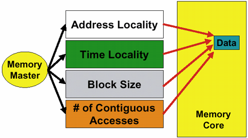
This is where Virtual Channel architecture comes into play. Virtual Channel Memory uses a set of high speed static registers (high speed memory) between the memory core and I/O pins (between the memory itself and its connection to the "outside world" or memory masters). These high speed registers provide each memory master with its own "Virtual Channel" to the SDRAM. This helps reduce latency and increase the efficiency of the amount of bandwidth available to your system as a whole.
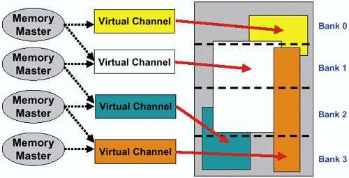
Specifically, VC-SDRAM features 16 virtual channels, each 128 bytes in width. The 16 channels are split evenly among the two internal banks each VC-SDRAM module features.
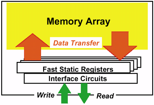
Unlike DDR-SDRAM, VC-SDRAM does not increase memory bandwidth by a fixed amount but it frees up bandwidth for use as a result of greater memory bus efficiency. NEC claims a figure of up to 90% efficiency, but that depends entirely on the number of memory masters accessing memory and the nature of each access.
At the same time, VC-SDRAM does not decrease latency by a fixed amount; rather, it depends on the nature of the accesses it decreases the latency for simultaneous accesses by multiple memory masters.
Theoretical Performance
Without discussing actual performance figures (those will be published in part 2 of this article) we can make some assumptions about the performance of VC-SDRAM.
In the event that a single memory master is requesting data from main memory, VC-SDRAM could potentially be slower than regular SDRAM since the memory master now has to go through a Virtual Channel to access the memory it would normally have direct access to. This performance hit should be negligible because of the high-speed nature of the Virtual Channels.
For regular business applications the performance improvement should be negligible.
The benefit of VCM architecture, specifically VC-SDRAM over regular SDRAM, will be seen when multiple memory masters are attempting to concurrently access the system memory. In this case overall system performance will be increased, and depending on how intense the memory accesses are the performance increase could be significant.
An application where a performance increase would be seen is in a 3D gaming environment where the CPU, AGP card, and sound card are all trying to access system memory at the same time. Applications that are memory streaming intensive or AGP texturing intensive will experience a performance benefit courtesy of VC-SDRAM.
Implementing VC-SDRAM
Unlike DDR-SDRAM, VC-SDRAM is pin compatible with SDRAM and is completely transparent to software. It does require chipset support which is provided for by both the Apollo Pro 133 and the Apollo Pro 133A, which is why VIA is pushing the standard. Micron has already begun shipping systems based on the Apollo Pro 133A using VC-SDRAM and they are currently the only major manufacturer to be shipping the new Pentium III 600B since both Dell and Gateway are waiting on Intel's i820 release before they can ship a 133MHz FSB system.
It is currently available in frequencies up to 143MHz which means it can be used in PC133 compliant systems, such as those built around the Apollo Pro 133/A. According to NEC there is no additional cost of ownership for VC-SDRAM, but at the same time this means that you can't move your VC-SDRAM with you if you decide to migrate to a platform that doesn't support VC-SDRAM. Also the availability of VC-SDRAM is currently limited, but it is in existence, so depending on the demand it may or may not grow to be a more popular solution.
Final Words
Tomorrow, we'll be taking a look at the performance of the Apollo Pro 133A with VC-SDRAM in various real world applications to see if the performance improvement is actually there. VC-SDRAM + Apollo Pro 133A could become a viable alternative to Intel's RDRAM + i820 move, and a much cheaper one.
Initial claims state that going down the RDRAM path adds up to $300 to the overall cost of a system. Keep in mind that these claims are coming from Micron, a company that is supporting their decision to go for VC-SDRAM + the Apollo Pro 133A, but one thing is for sure -- RDRAM won't be cheap once it hits.
Unless DDR-SDRAM becomes a quick reality, RDRAM will probably be the trend Intel pushes the market towards and, although it won't be cheap at first, it will most definitely become more affordable. But what solution do you have between the time that it isn't affordable and the time that it becomes so? The Apollo Pro 133A is an option. However, wait until tomorrow before deciding on whether or not the real world performance supports or refutes that argument.


