Original Link: https://www.anandtech.com/show/13245/hot-chips-2018-nvidia-xavier-soc-live-blog
Hot Chips 2018: NVIDIA Xavier SoC Live Blog (5pm PT, Midnight UTC)
by Ian Cutress on August 20, 2018 7:55 PM EST- Posted in
- Hot Chips
- Trade Shows
- SoCs
- NVIDIA
- Live Blog
- Xavier
- Automotive
07:55PM EDT - NVIDIA has a couple of talks during Hot Chips, with this first one going into the Xavier SoC.
07:57PM EDT - Leading architect of Xavier
07:57PM EDT - Compute has become more accessible
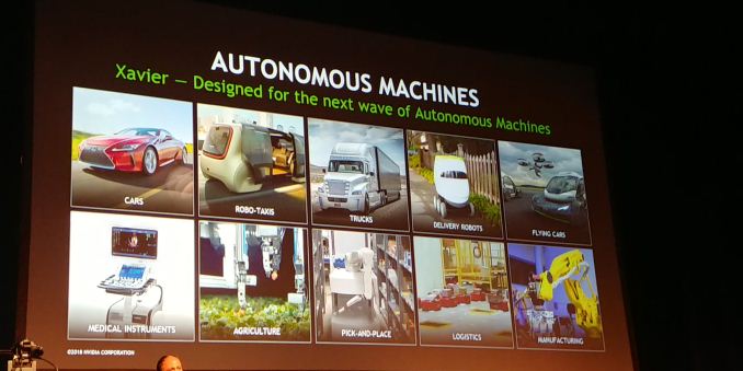
07:57PM EDT - What do we need in an autonomous machine chip
07:57PM EDT - Need 10s of Tera-Ops of CV and compute perf
07:58PM EDT - Goal to build a chip to fit in these markets and fit in the power targets
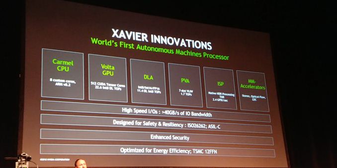
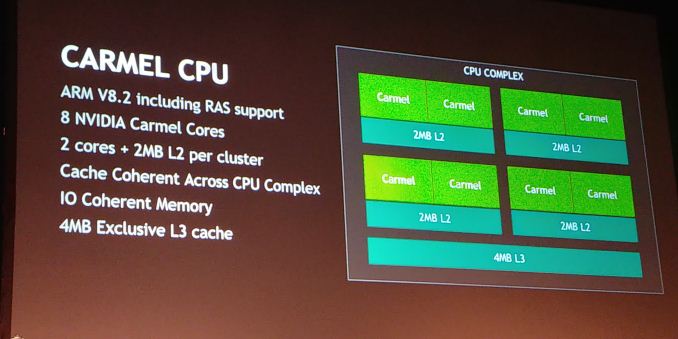
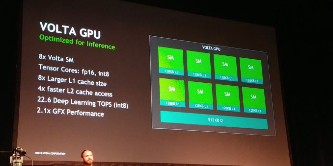
07:58PM EDT - 8 custom Carmel cores, 512 CUDA Volta cores
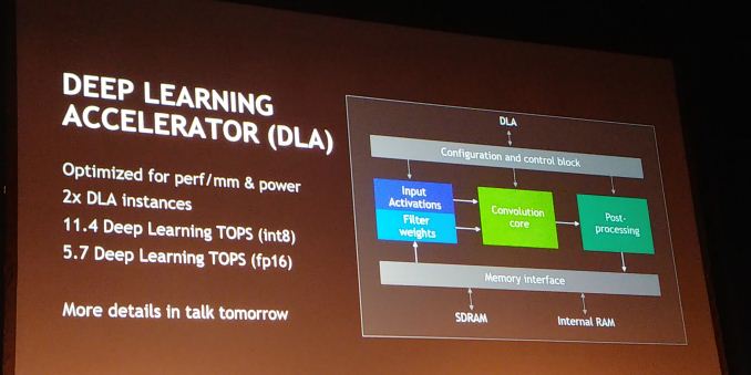
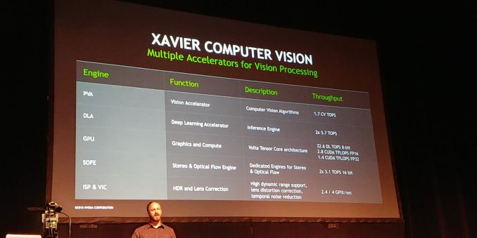
07:59PM EDT - fixed function accelerators: Deep Learning Accelerator (11.4 DL int8 TOPS)
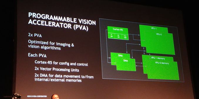
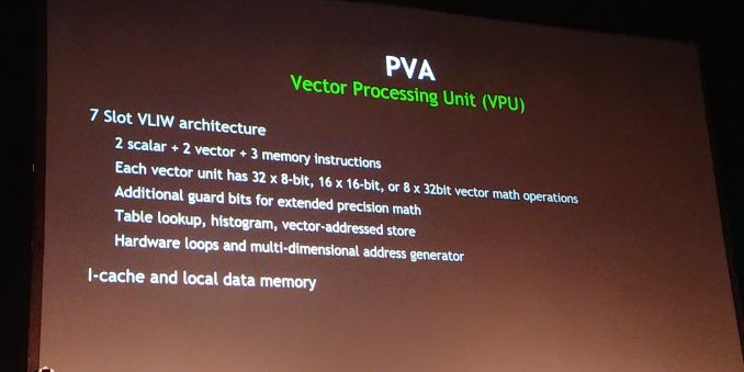
07:59PM EDT - PVA (Programmable Vision Accelerator) 7-slot VLIW, 1.7 TOPs
07:59PM EDT - ISP - needs to be native HDR
08:00PM EDT - rearchitected from Tegra
08:00PM EDT - higher precision math for HDR
08:00PM EDT - DLA and PVA are for certain compute aspects which can appear
08:00PM EDT - other multimedia accelerators (stereo, optical flow)
08:00PM EDT - supports high-speed IO
08:00PM EDT - ASIL-C compliant, ISO26262
08:01PM EDT - Comes through dev processes
08:01PM EDT - TSMC 12 FFN
08:01PM EDT - ECC and parity thoughout RAMs, some level of redundancy
08:01PM EDT - Units optimized for energy efficiency
08:02PM EDT - Optimized differently than desktop GPU
08:02PM EDT - Design started 4 years ago
08:02PM EDT - 9B transistors, 350 mm2
08:02PM EDT - 8 Carmel cores
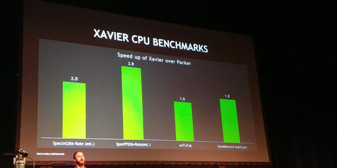
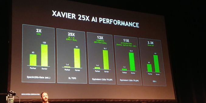
08:03PM EDT - Speedup vs Parker
08:03PM EDT - 2.0x on SpecInt 2k6
08:04PM EDT - Volta optimized for inference
08:04PM EDT - Tensor cores, fp16, int8 at 2x of fp16
08:04PM EDT - 128KB L1 per SM, 512KB of shared L2
08:05PM EDT - Two DLAs in the SoC
08:05PM EDT - Optimized for perf/mm and power
08:05PM EDT - More in talk tomorrow
08:05PM EDT - NVDLA
08:05PM EDT - PVA uses Cortex-R5
08:06PM EDT - Each PVA (two in chip) has a Cortex R5, two Vector Pipes, each pipe has its own DMA and own memory
08:06PM EDT - 7 wide VLIW in each PVA
08:06PM EDT - each Vector Unit can do 32 x 8-bit or 8 x 32-bit vector math
08:07PM EDT - Vector unit has its own I-cache and local data
08:07PM EDT - secret sauce for hardware looping and address generation
08:07PM EDT - Works on tiles of memory
08:07PM EDT - DMA works on addresses to keep it fed
08:08PM EDT - Lots of pipes to remove workload from the GPU at lower power
08:08PM EDT - Xavier has 25x AI perf over Parker
08:08PM EDT - due to DLA support
08:09PM EDT - lens distortion correction hardware
08:09PM EDT - 256-bit LPDDR4X
08:09PM EDT - (he said LPDDR5 first... so next gen?)
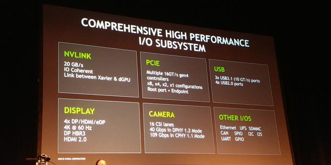
08:10PM EDT - Xavier has 20 GB/s NVLink, multiple PCIe Gen 4.0 controllers
08:10PM EDT - 3 x USB 3.1 ports (says 10 GT/s, not 10 Gbps ?)
08:10PM EDT - supports 4x displays, HBR3, HDMI 2.0
08:11PM EDT - Cameras - 16 CSI lanes, 40 Gbps in DPHY 1.2, 109 Gbps in CPHY 1.1
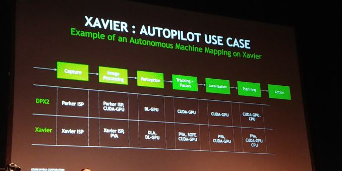
08:12PM EDT - Autonomous vehicles use case
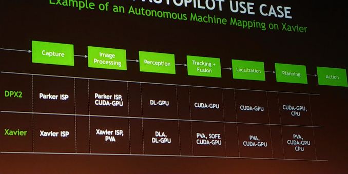
08:12PM EDT - In Parker, most things mapped to the GPU
08:13PM EDT - In Xavier, lots of offload
08:14PM EDT - Almost all segments can be accelerated by PVA
08:14PM EDT - DLA in perception
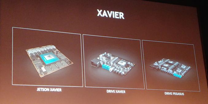
08:16PM EDT - Xavier scales from Jetson up to Pegasus
08:16PM EDT - Time for Q&A
08:17PM EDT - Q: What protection on the memory bus? A: ECC implemented through the bus, no extra bits
08:17PM EDT - That's a wrap. Next talk is about Microsoft Azure Sphere: https://www.anandtech.com/show/13246

