Original Link: https://www.anandtech.com/show/10025/examining-soft-machines-architecture-visc-ipc
Examining Soft Machines' Architecture: An Element of VISC to Improving IPC
by Ian Cutress on February 12, 2016 8:00 AM EST- Posted in
- CPUs
- Arm
- x86
- Architecture
- Soft Machines
- IPC
Last week, Soft Machines announced that their 'VISC' architecture was available for licensing, following the announcement of the original concepts over a year ago. VISC, in a nutshell, is designed as a solution to improving the number of instructions per clock a single thread can process in a given time, which potentially makes it a very interesting design in an era where IPC gains are harder and harder to realize.
The concepts behind their new ‘VISC’ architecture, which splits the workload of a single linear thread across multiple cores, are intriguing and exciting. But as with any new fundamental change in computer processing, subject to a large barrage of questions. We were invited to a presentation and call with the President and Chief Technical Officer Mohammed Abdallah and the VP Marketing and Business Mark Casey, and I put a number of questions on the lips of analysts to them.
Identifying Single Thread Performance Bottlenecks
Any discussion about processor performance over the last couple of decades has involved several factors, including getting better performance through an increased power budget, a higher frequency, extracting instruction level parallelism (ILP), getting better at minimizing delays through better branch prediction, or adding more cores and improving thread level parallelism (TLP). Each of these methods have varying degrees of success at increasing performance – long-time readers will remember the Pentium 4 days of hitting a frequency and power wall which then switched the focus to efficiency. Some tasks, like graphics, are inherently parallel and can take advantage of multiple hundreds or thousands of cores, or the software can be optimized. However, the nature of most software code and instructions is that they are single threaded by nature, and their performance relies on how fast the instructions can be processed within a single thread.
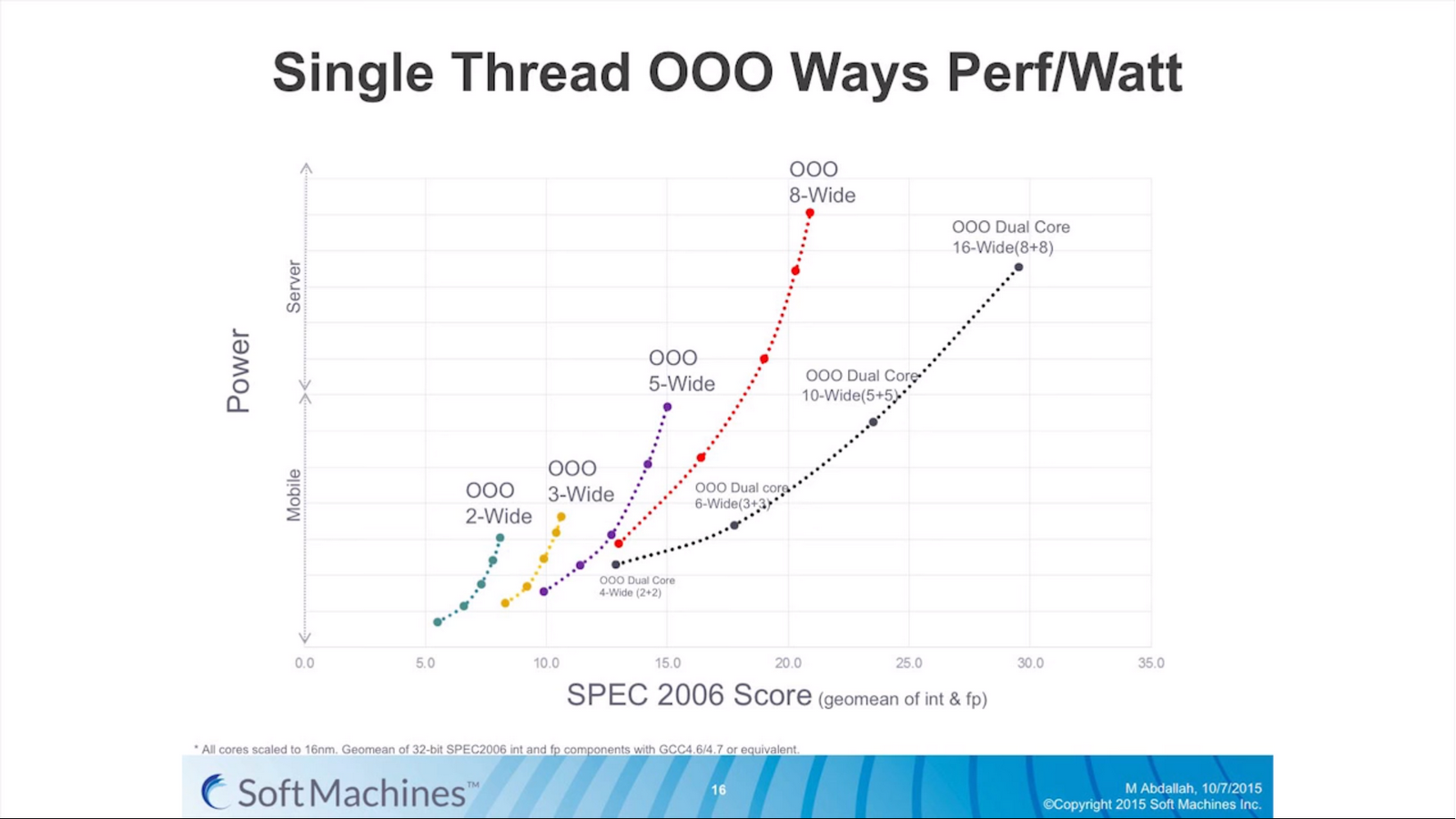
The main way of increasing performance, or in this case the instructions per unit frequency (instructions per clock, or IPC), is to expand the CPU architecture to allow more commands to be processed at once. Moving from a 3-wide out-of-order architecture to a 5-wide out-of-order architecture theoretically allows for a 66% increase in instruction throughput if (and only if) the code is sufficiently dense enough to extract those operations, and the other features in the architecture can ensure all the operations are fed every clock cycle.
The problem with moving to a wider architecture is typically power and design complexity. As shown by various chip designs over the years, the wider the architecture the more silicon has to be set aside for assets like buffers, re-order windows and caching. If there is a silicon budget and enough power headroom, we see designs like the six-wide Intel Skylake cores or the seven wide NVIDIA Denver cores able to extract peak performance when code is written that matches the hardware. However the potential downside of a wide architecture is that it remains inefficient for sets of instructions that only need a 2-wide or a 3-wide architecture. Alternatively, if multiple programs or threads want to use the hardware, then a single core is inaccessible to additional threads while the first thread is still in use (though this can be avoided somewhat by simultaneous multithreading or SMT which will let another thread have access when the first has encountered a stall such as waiting for L1/L2 memory).
As a result, modern designs also include a number of cores to handle the multile thread/multiple program scenario. Generally speaking this works well, especially with high-performance cores, but it becomes a bit of an issue itself when much of the world’s hardware is actually composed of many cores that have poor single threaded performance. Older Core 2 / Conroe systems, basic Bulldozer, or ARM Cortex-A7 designs are (still) widely used and often ship with multiple cores to allow for multiple programs at once. And while they can scale up with additional threads to the number of cores they offer, if any single or lightly-threaded software needs more performance, those extra cores are not used or are only minimally beneficial overall.
This brings us to Soft Machines, whose VISC architecture aims to change this.
Meet VISC
I should start by saying that despite the similarities to other architectural names, VISC is not an acronym. I asked directly and it is merely a noun for the purposes of trademarking. People can interpret it as a ‘virtual instruction set computing’ or something similar, but the company doesn’t apply any acronym to the letters.
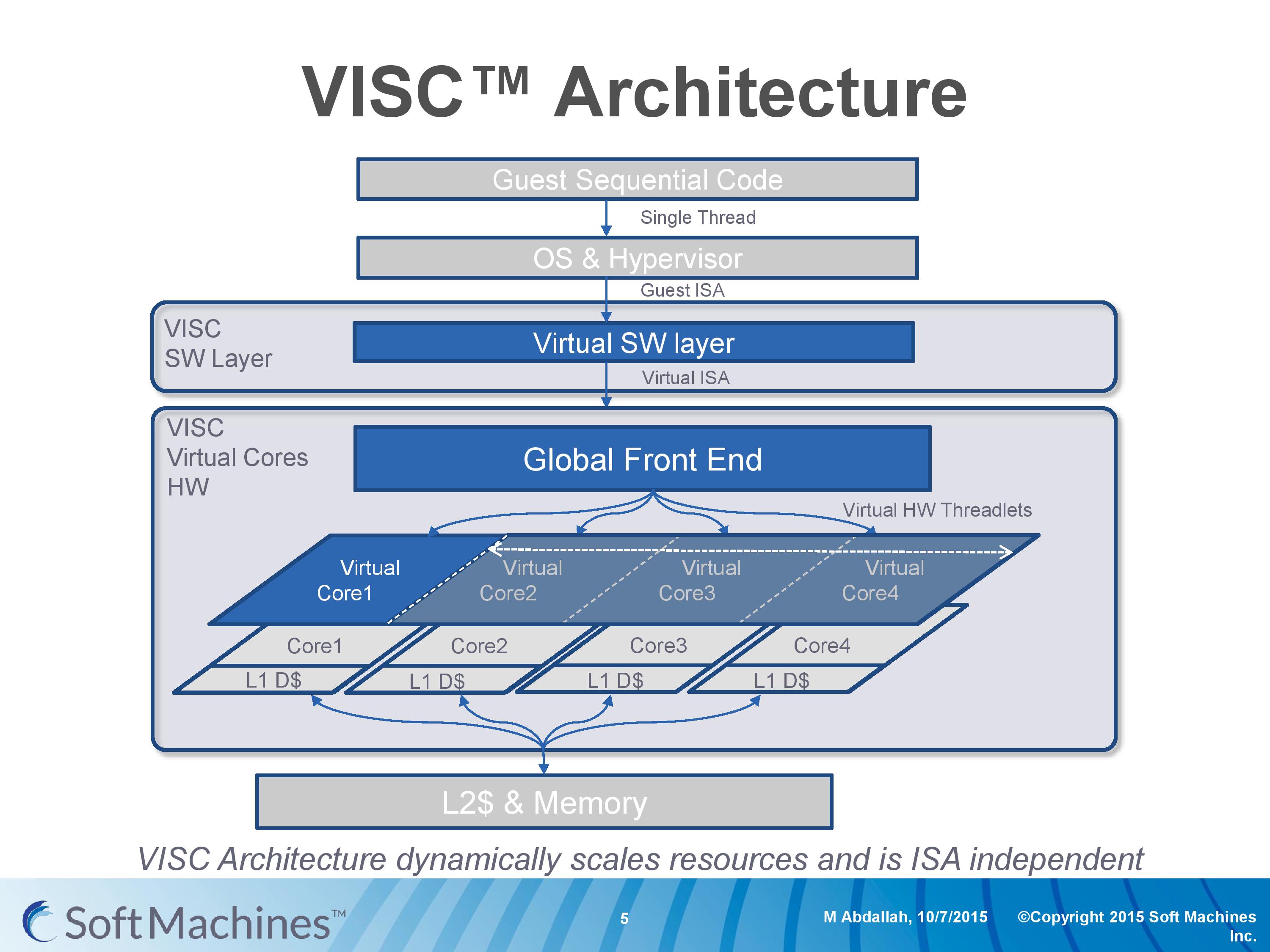
But a virtual instruction set is a good description here. For the most part, processor architectures were traditionally built around either CISC (complex) or RISC (reduced) instruction sets and execution models, while more modern designs (e.g. Intel Core) are increasingly a mix, or so-called ‘CRISC’ design. The difference between CISC and RISC boils down to the fact that simpler designs can be more power efficient, but complex designs can do more complicated things in fewer cycles, all the while CRISC essentially meets the two paradigms in the middle in an attempt to gain the benefits of both, though not without inheriting some of the drawbacks as well. VISC, for lack of a better description, is a RISC design using a custom instruction set over a translation layer which allows a single thread of operations to be dispatched over multiple physical cores. The base diagram looks something like this:
Here is an example of a VISC design with four physical cores. The design can handle four ‘virtual cores’ or threads as well, but what makes the VISC design different is that when the virtual core has a thread of instructions, it can use the resources of any physical core. Thus, if each physical core is a 4-wide out-of-order design, if a thread running on a virtual core can utilize the resources of all four cores essentially making a giant 16-wide design, then under VISC can do so.
This should instantly throw up a number of questions on ‘What!? How?! Why?! Power? Frequency? Performance? Efficiency? Complexity?’ and as well as many others in the industry, we had the same questions.
The VISC Instruction Set and Global Front End
Common instruction set architectures (ISAs) such as x86, ARMv8, Power, SPARC and other more esoteric ones rely on system code converting into predefined instructions that each design can handle. VISC comes with its own ISA as well, separate from the others, which VISC cores and virtual cores use. When using native VISC code, the global front end will split the instructions into smaller ‘virtual hardware threadlets’ which are then dispatched to separate virtual cores. These virtual cores can then issue them to the available resources on any of the physical cores and keep track of where the data goes. Multiple virtual cores can push threadlets into the reorder buffer of a single physical core, which can split partial instructions and data from multiple threadlets through the execution ports at the same time. We were told that each ‘virtual core’ keeps track of the position of the relative output.
The true kicker (and so much of what sets VISC apart) is that when multiple virtual cores are in flight at one time, the core design allows the virtual core allocation of resources to be dynamic on a near-single cycle latency level (we were told from 1-4 cycles depending on the change in allocation). Thus if two virtual cores are competing for resources, there are appropriate algorithms in place to determine what resources are allocated where.
One big area of focus in optimizing processor designs for single-thread performance is speculation – being able to deal with branches in code and/or prefetch relevant data from memory when needed. Typically when speculation occurs, as the data for a single thread is contained within a core, it is easy enough to deal with code paths that rely on previous data or end up with bad speculation.
In the virtual core scenario however this becomes trickier. VISC tackles this in two ways – firstly, the threadlet generation is designed to minimize cross-core communication because this adds latency and reduces performance. Second, each core can communicate through either the register file or the L1 data caches. The register files have a single cycle latency for data but can only transmit tens of values, whereas the L1 cache has a 4-cycle latency but can transmit thousands of values.
Typically communicating through a register file is seen as a risky maneuver and difficult to control, especially when you have multiple physical cores and each core needs each other core to be able to place/take data into the right registers. Soft Machines told us that a large part of their design work has been in this area of speculation and data transfer. Specifically on speculation and branch prediction, we postulated that they were over ten years behind Intel in this, and the response we got was in a similar vein, stating that using Intel’s branch prediction methods could offer at least 20-30% better performance with branching code. However, we were told that the VISC design is quicker to recover in the event of a failed branch, needing only a few cycles.
The Pipeline
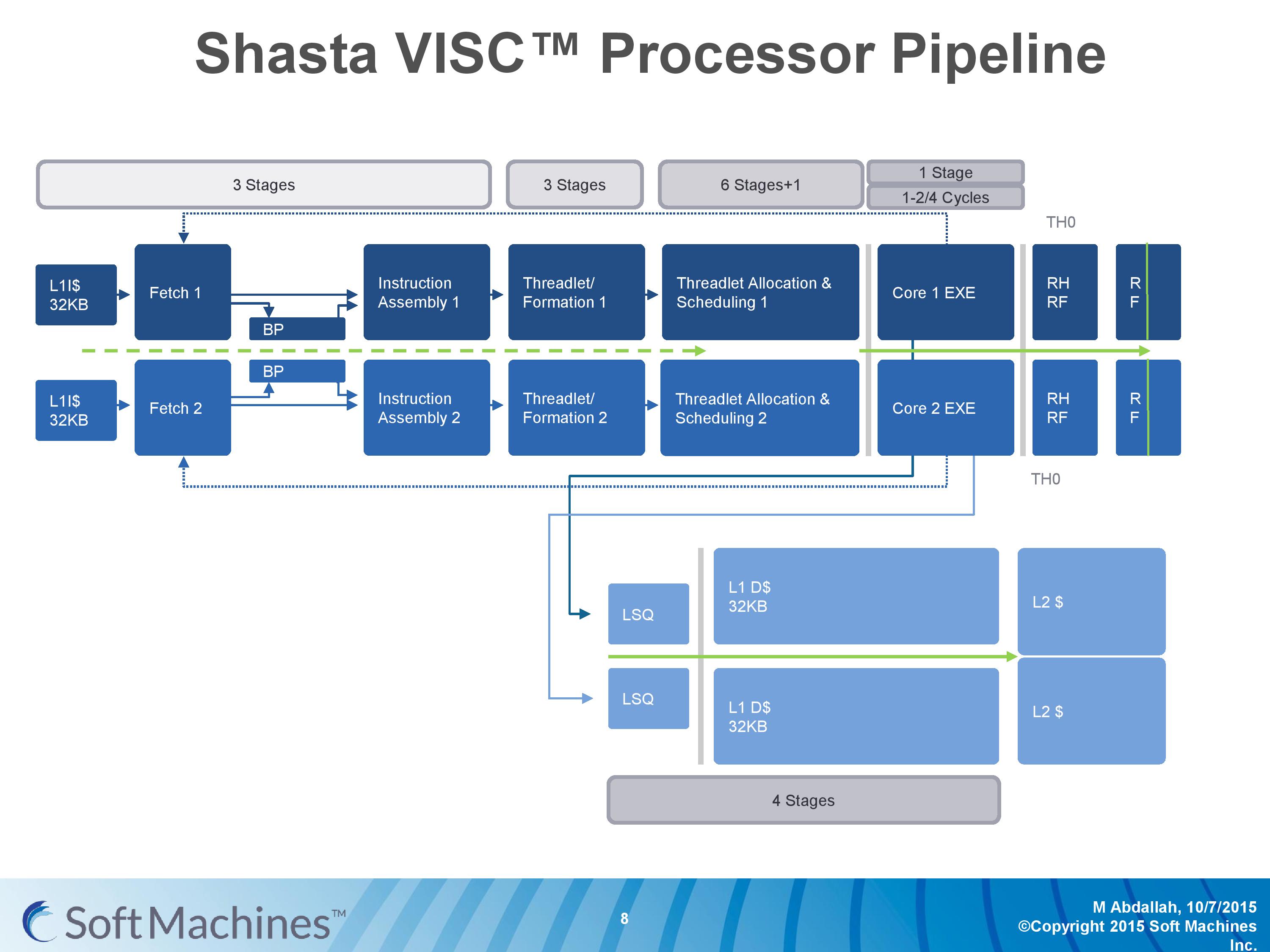
The first VISC core available for license is Shasta, a dual core part that enables up to two virtual cores or threads (2C/2VC), and we were given a base overview of the pipeline.
Normally we would see a pipeline of one core but this is a pipeline of both cores of Shasta. This pipeline, compared to the original VISC prototype, is also deeper. The pipeline looks relatively normal to others to start, where the thread either takes an instruction or issues a fetch for data into the instruction assembly. Making the VISC instructions and data into threadlets takes another three stages, but the allocation and scheduling takes six (plus one). On that subject, Soft Machines mentioned that keeping track of data across multiple cores per virtual core is tricky, as well as dealing with reorder buffers and parallel instruction management, that’s why there are a large amount of stages here. The plus one goes back to variable physical core allocation methodology, ensuring that if there are two threads active that the heavier one will get the most resources. The threadlets are then executed on the ports of each core, with a possible 1-4 cycle delay if data needs to be transferred across the core boundaries via registers or L1 cache.
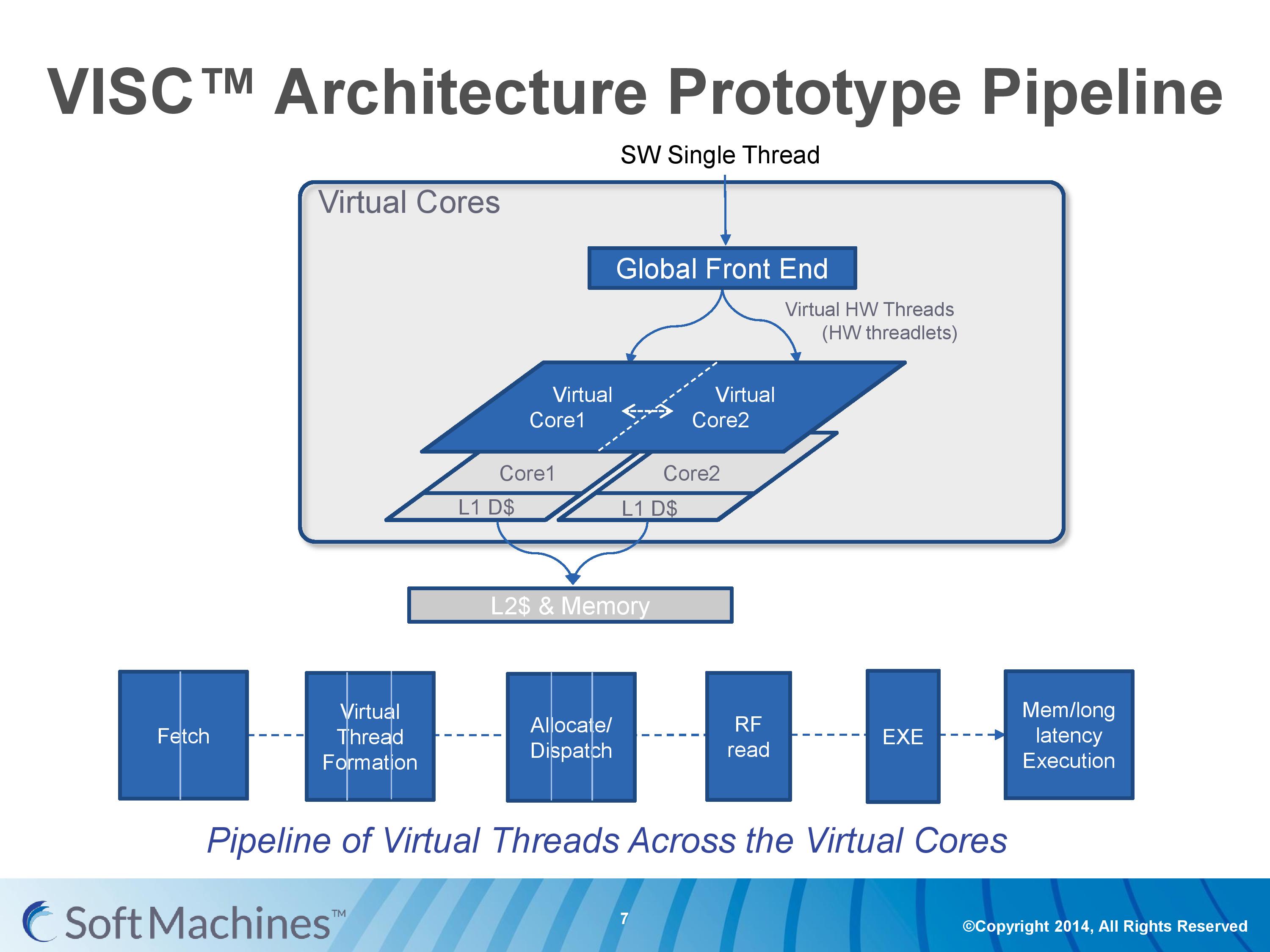
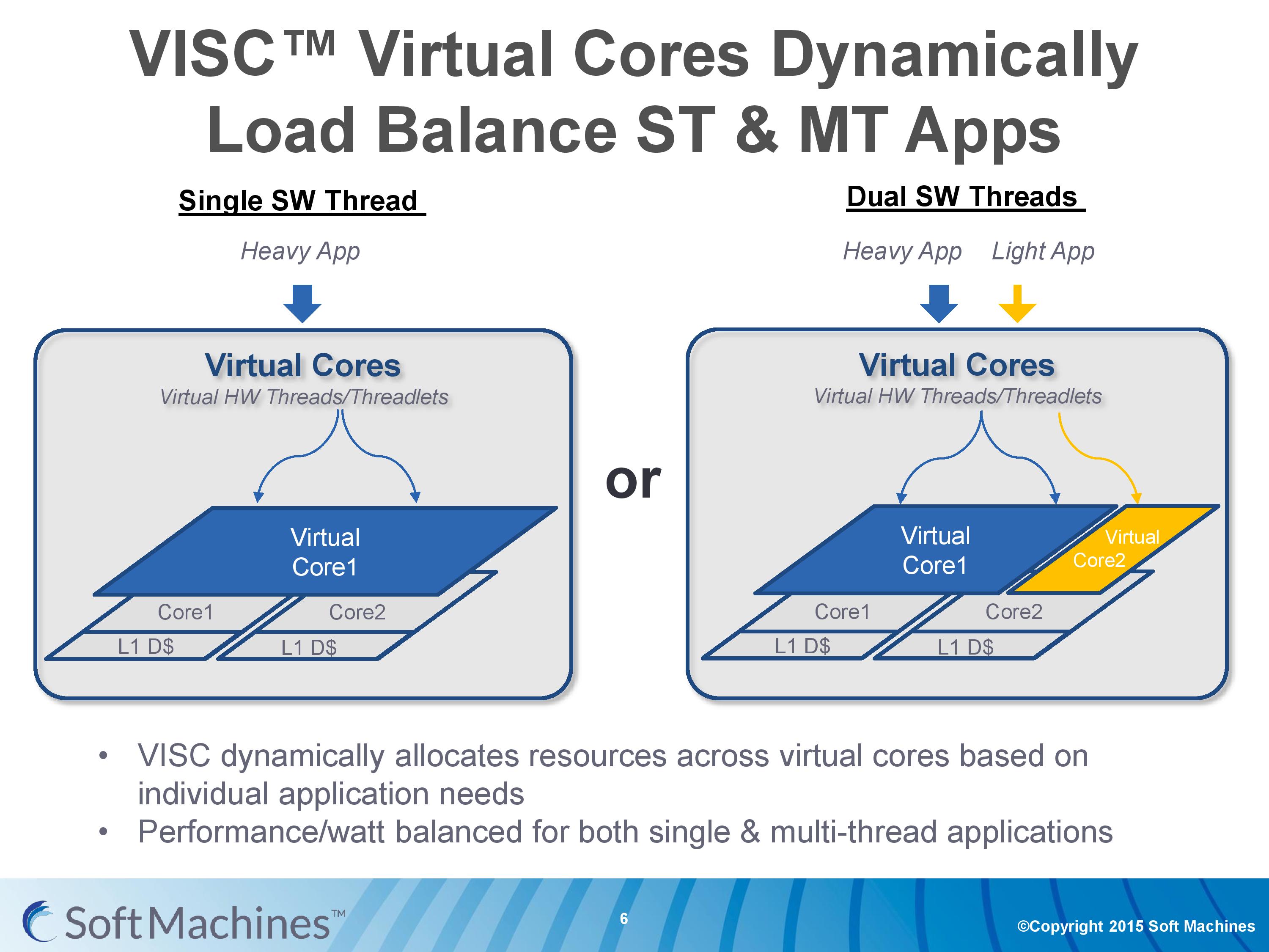
With the variable allocation of fractions of a core to a virtual core, VISC is designed for this situation:
If one heaver thread needs more resources, it can take them from idle ports on a second core (or third, or fourth). The virtual cores can be configured at the software stage as well to limit their use (e.g. keep a VC to half a physical core), and this can be configured at runtime at the expense of 10-12 cycles. There is a quality of service implementation as well, so if a virtual core takes a high priority thread, it will have access to more resources by default.
Dealing with Guest ISAs and a Translation Layer
Going back to this architecture diagram, everything up to the global front end is another interesting story as well.
Part of Soft Machines' product package is a low level virtual software layer that will translate a guest instruction set and convert it into the VISC ISA. This is to allow VISC to be used with existing software, and to more easily integrate into current environments rather than trying to establish an ecosystem for a new architecture in 2016. Soft Machines tells us that two instruction sets are supported, one of which will be ARMv8. It was implied that x86 would be the other, although they were reluctant to outright confirm it (ed: x86 translation is likely not to be looked upon fondly by Intel). Meanwhile we were told that writing additional translation layers, while not trivial, can be done and that they plan to support other guest ISAs in future.
So for all intents and purposes, this is a translation layer converting from ARMv8 to VISC. Many companies over the past couple of decades have tried with translation layers – Intel with Itanium, Transmeta to x86, and one of the latest was NVIDIA with Denver, which translated ARM to a custom ISA. Mentioning Itanium, Transmeta and Denver, for those who have followed the industry, might bring a chill down the spine given the very limited success each of these platforms have had. Soft Machines’ CEO was keen to point out that the purpose of the translation layer for VISC is very different to these previous attempts.
The VISC translation layer is designed to be a thin and lean implementation whose main role is to maintain compatibility to the VISC ISA, not to extract performance. Taking Denver as the most recent example, the translation layer there is designed to adjust the ARM instructions into Denver’s ISA and extract instruction level parallelism into the 7-wide design. For VISC, we are told, there is no need to go after performance at this level. The main point at which the VISC design increases performance is at threadlet generation, not in translation and making instruction sequences better fit the VISC hardware. This allows the ARM translation layer to have a less than 5% overhead, according to Soft Machines, and releases a point of contention with previous translation layer designs. As long as the translation layer is 100% compatible, the performance can in principle be extracted at the threadlet level.
This also means, again according to Soft Machines, that any specific compiler enhancement offered by others can also be used when translated. We put it to them that in the case of x86 certain codes are accelerated better on Intel’s compiler than say GCC (a question that arose out of the results we’ll go into later), and we were told that those instruction enhancements by ICC should translate well into the VISC ISA after going through the translation layer.
We asked about the VISC ISA, but were told that more information about this and the core design would be released at a later date as designs progress. We were told that it is a relatively small ISA (as to us sounds like a RISC, which is easier to extract ILP at lower power) with smaller instructions in comparison to ARM and x86. I would assume that this means they are fixed length, but this was not confirmed.
Soft Machines
To put it succinctly, having a thread take resources from multiple cores - when the performance can be extracted - sounds like the long-desired solution to the problem making multi-core designs more useful in lightly-threaded scenarios. Having multiple threads use resources on a single core on the same clock cycle is an even bigger leap in the same direction. Now obviously Soft Machines didn’t come up with this overnight.
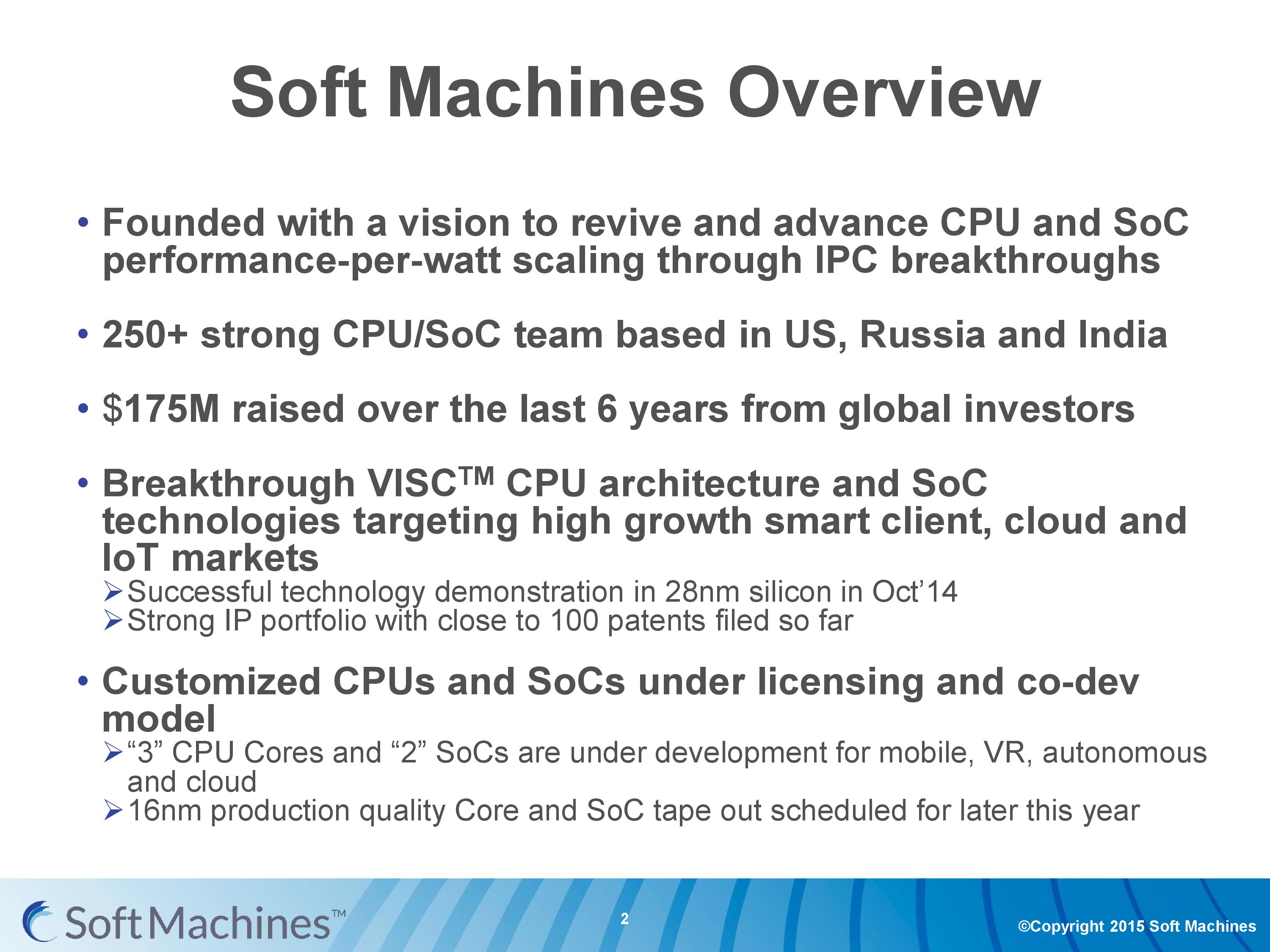
Soft Machines came out of stealth mode at the 2014 Linley Conference. Their main goal was to increase performance-per-watt using better IPC designs, which is often one of the better ways if you can keep a design fed with data. One big challenge to this is that IPC has been somewhat flat these past few years - we're seeing small sub-10% yearly increases from the big players using standard designs. Soft Machines were already six years old at the time, with $150M+ raised from investors that include Samsung Ventures, GlobalFoundries, AMD, Mubadala and others (with another $25M since). If those names all seem interlinked, it’s because they all have historic business or investment dealings with each other (AMD/GloFo, Samsung/GloFo, AMD/Mubadala etc.). The team at Soft Machines is 250+ strong, with ex Intel, ex Qualcomm, ex AMD engineers on staff from processor design to platform architects. Half the staff is currently located in California.
At the 2014 conference, aside from explaining what they were doing, Soft Machines also exhibited working silicon of their design. The first generation proof of concept was fabbed at 28nm at TSMC and running at 500 MHz.
It seems odd to say that it was done at TSMC, especially with Samsung and Global Foundries as investors. We were told that this was due to timing and positioning with IP more than anything else, and the same is true for the next generation at 16nm FF+, rather than 14nm.
VISC and Roadmaps
The first generation chip wasn’t perfect – there were some design flaws in silicon that required specific workarounds relating to cache flushing and various methods, but at the time it was compared to a single thread Cortex A15 running at a similar frequency in a Samsung processor. The results with SPEC2000, SPEC2006, Denbench and Kraken gave a corresponding IPC relative to A15 of 1.5x to 7x, or as Soft Machines likes to put it: 3-4x "on average." It was estimated that access to a second physical core improves performance by an average of 50-60%, or an average IPC of 1.3 per core compared to 0.71 for Cortex A15, which explains the 3-4x average.
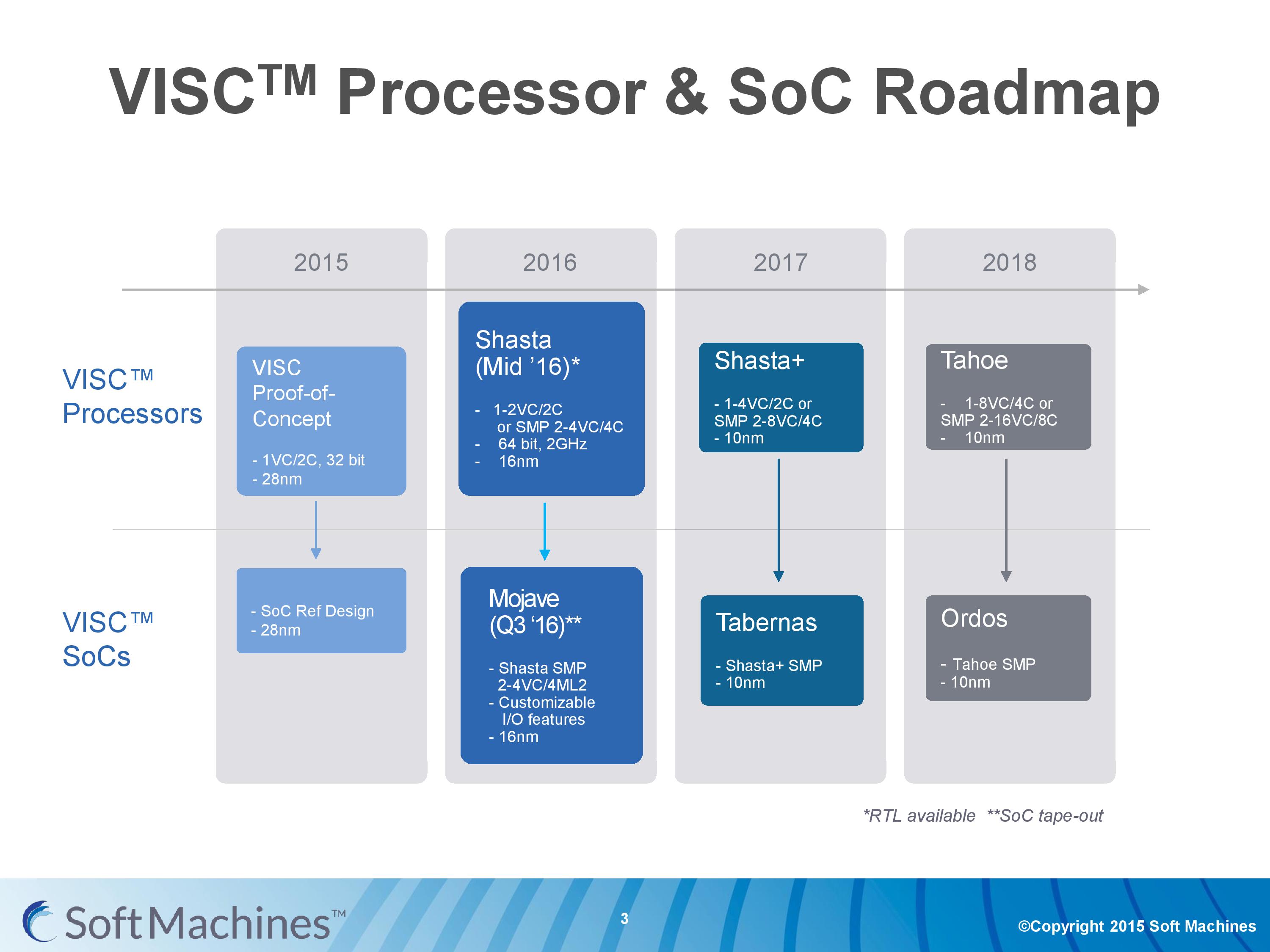
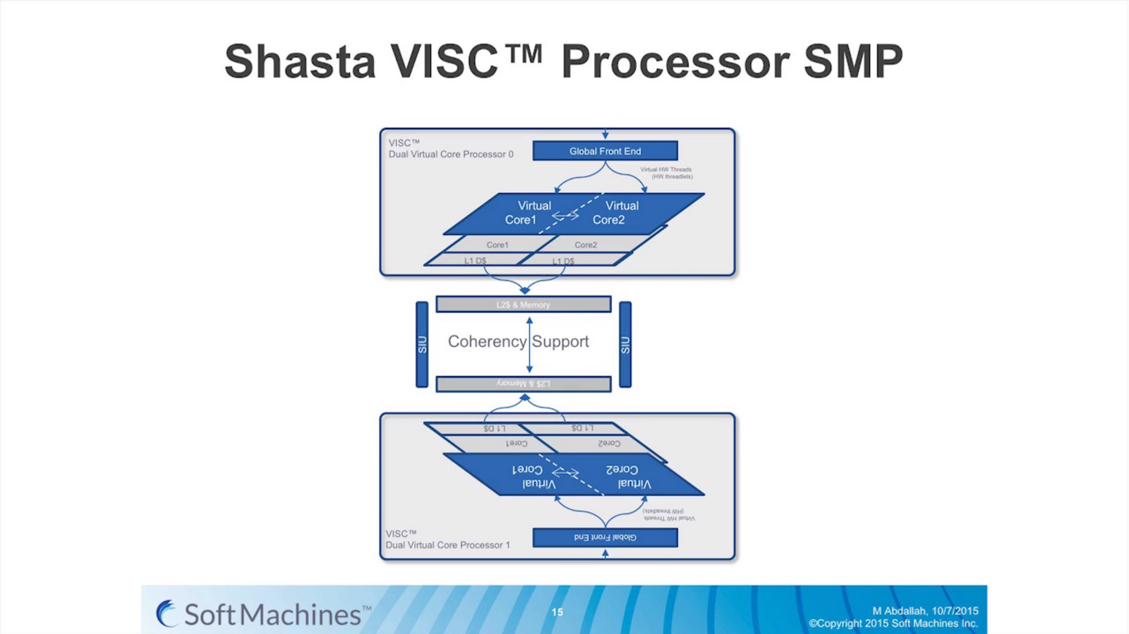
The roadmap for Soft Machines put their second generation VISC core, Shasta, in line for 2016. It was formally announced at the 2015 Linley Conference, with this month’s announcement being more about availability for licensing on 16FF+. The Shasta core on this node is designed as a 2C/2VC design, or two of these can be put together using a custom protocol interconnect to form a dual 2C/2VC design.
The custom interconnect fabric here is capable of over 200 GB/s, although in current designs only a single interface is present, allowing only two chips to be connected.
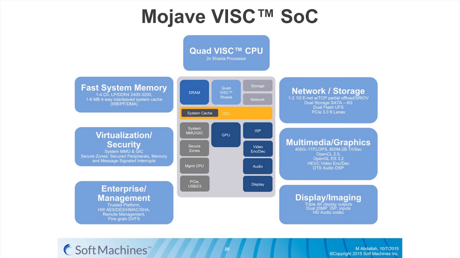
The dual processor design is going to be part of the Mojave IP as a fully integrated SoC.
Along with the requisite VISC cores, the Mojave SoC includes PowerVR graphics, a DDR4 memory controller, virtualization management, a PCIe root complex capable of eight lanes of PCIe 3.0, USB ports, support for SATA, UFS, OpenCL 2.0 and other standards.
Looking forward, Soft Machines would like to see production move to 10nm in 2017 to take advantage of further power and area scaling. Meanwhile along that same timeframe they also want to expand the Shasta design to allow for four virtual cores per two physical cores, essentially allowing more threads to be in flight at one time and fully use the resources better. 2018 sees the move to four physical cores and eight virtual cores per design, while still supporting SMP and SoC designs as well.
The Data: Soft Machines' Proof
Ever since the initial announcement of the VISC architecture in 2014 there has been a element of it sounding too good to be true, and Soft Machines' 2016 announcements have come with yet more questions as well. Aside from questions requiring more information about the architecture and ISA, the big money questions relate to performance. We mentioned a couple of pages back that the original 28nm design made its way to silicon at 500 MHz and was shown as a proof of concept. At the 2014 conference, the platform was compared to both ARM and x86 and offered better scores on Denbench compared to both while also using less power. Now that Shasta is on the 16nm node, the big question is how the new design at a 2 GHz frequency compares, and if the increase in frequency has upset some of the IPC gains.
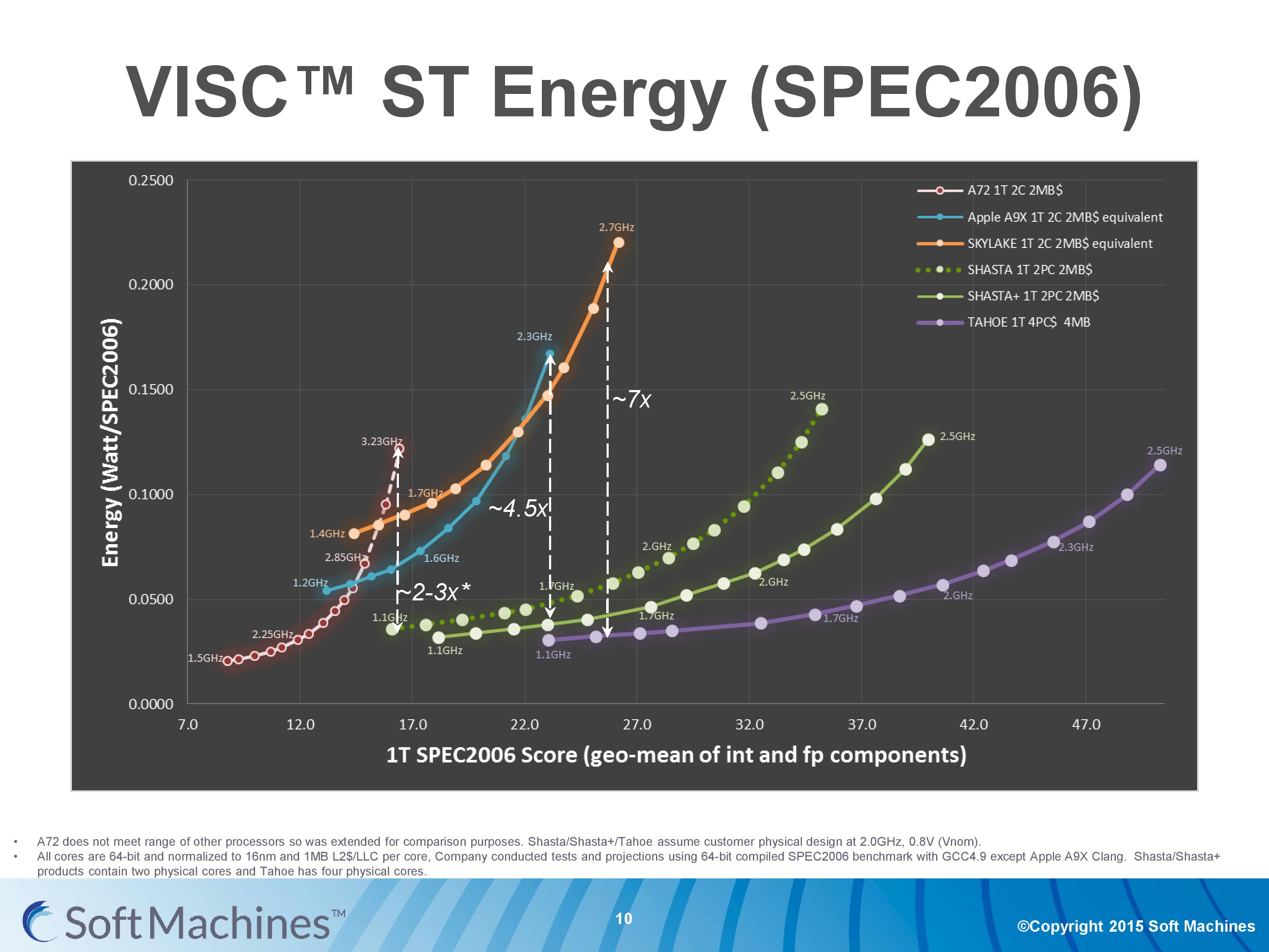
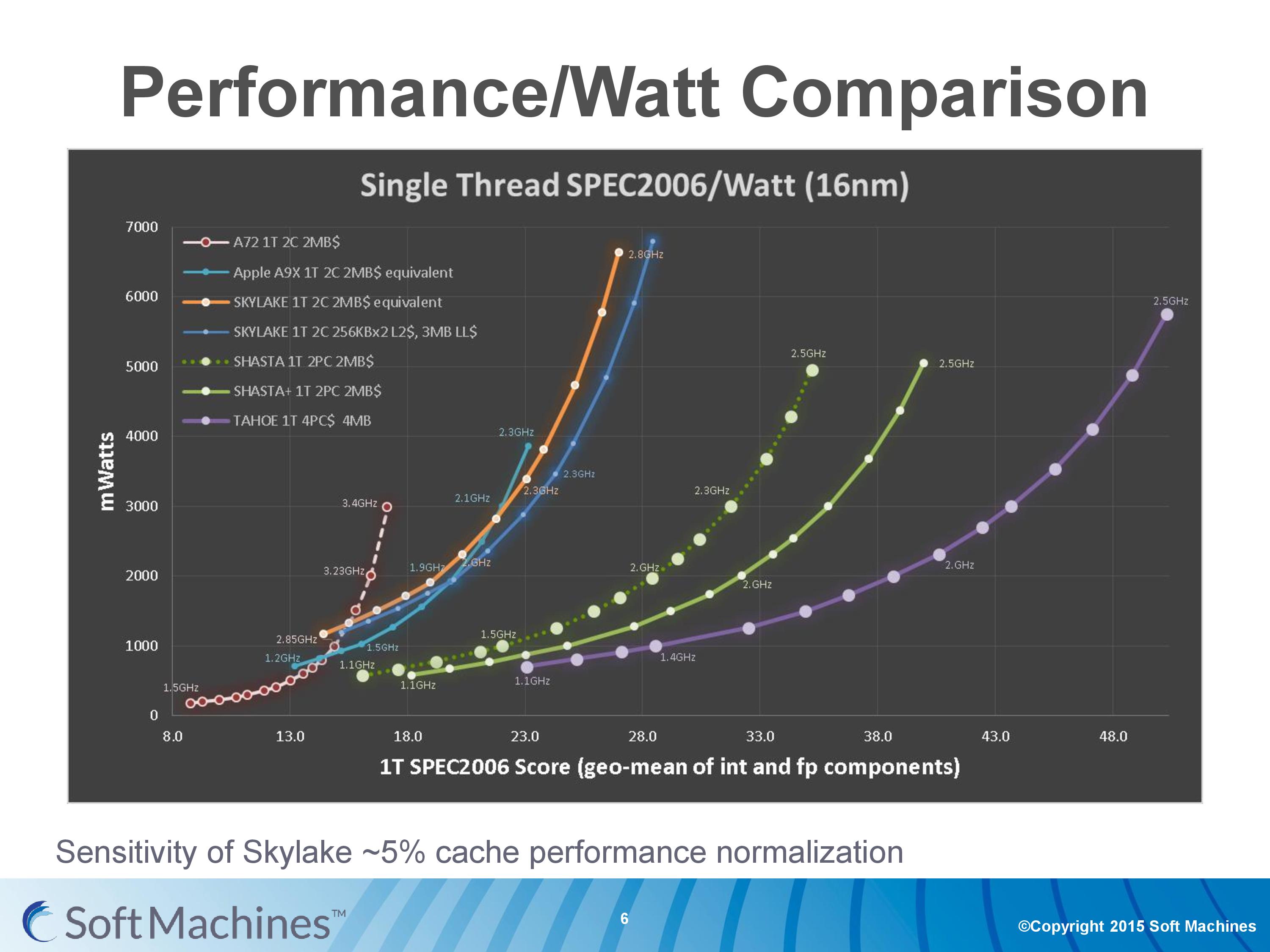
So it’s at this point that we have to show this graph before we can progress any further. This is a graph which has caused a lot of commotion among the analyst community, because it can be a very difficult graph to digest and work out what is going on. I’ll take you through it. But to start, ignore the vertical dashed lines.
This is a graph from Soft Machines attempting to show the efficiency of several CPUs cores: Cortex-A72, Apple’s Twister (A9X), Skylake, Shasta, Shasta+ (2017), and Tahoe (2018). It is a graph of the average power consumed per unit SPEC2006 score plotted against the SPEC2006 score, and each dot on a line shows the relative score of each CPU at a given frequency.
The reason why this graph has caused a lot of commotion is that it shows a lot of data based on a lot of assumptions displayed in a very odd way. The following points are worth mentioning
| The Scores #1 | This graph shows the geometric mean of SPEC2006int and SPEC2006fp, the integer and floating point parts of the SPEC2006 set of benchmark tools. Because different architectures focus on integer and floating point performance to differing degrees (more units focused on INT or FP), these results are typically given separately, with individual subtest scores. Practically no-one in the industry puts them together as a geometric mean, which has some analysts wondering if there are certain subtests where VISC scores particularly low. |
| The Scores #2 | This graph shows only single threaded results, even though each CPU is listed as having two cores in the data but running a single thread. This puts the Soft Machines cores in the best light, as a single thread has access to all the ports on two cores as well as two re-order buffers and two cores' worth of L2 cache. |
| Conversion #1 | All the results have been converted as if each CPU design has 1MB of last level cache per core. This means that designs such as the A9X and Skylake CPUs have been reduced, and scores have been adjusted by ambiguous ‘industry standard techniques’ according to SMI. A number of analysts say that this is not a fair conversion, as an A9X core or Skylake core with less cache would be arranged differently in silicon to take advantage of more space for other things or lower latencies. |
| Conversion #2 | All the results have been converted to 16nm FinFET+ on TSMC, again by ‘industry standard techniques’. This is a hard one to grasp, because core designs are not simply ‘shrunk’ from one node to another. Similar to the cache situation, each process node can be optimized for metal layers and arrangement for latency and bandwidth optimizations. Each conversion, such as Intel’s 14nm to TSMC 16nm, or TSMC’s 28nm -> 16nm, would have to be thoroughly examined. Extrapolating from 28nm to 16nm would be an exasperating task to be accurate (and this level of extrapolation wouldn’t be acceptable even in a high school classroom as I pointed out). |
| Testing #1 | Not all points on the graph come from direct data. Each line has had several points taken from data and the rest are interpolated given basic power formulas. |
| Testing #2 | The platforms used are not all what they appear to be. So for example, the best Cortex-A72 16nm data point would be the Kirin 950 in the Huawei Mate 8, but instead a dual A72 was used from the Amazon Fire TV which as a 28nm MediaTek MT8173 running at 1.98 GHz. One could argue that A72 is new enough and only recently on 28nm that it isn’t fully optimized for the process yet and this is probably a low end version of that silicon. The Apple A9X numbers are actually taken from a 14nm A9 and the assumption was made that the dynamic power in a cold environment was similar to the A9X. The Skylake numbers were a mid-range Core i5-6200U in a Dell laptop, which could be prone to variable turbo modes or overheating, and that specific SKU is hardly the most power efficient model in Intel’s Skylake lineup. |
| Compilers | In order to ‘normalize’ the data, each of the actual data points taken were as a result of SPEC2006 being compiled on GCC 4.9 (or Clang for Apple). Typically for SPEC we normally consider the peak numbers possible with the best compiler, and as pointed out by some analysts, Intel’s results on their compiler can get scores more than double that of GCC, which can put a negative bent on Intel’s numbers. |
| Simulations | Almost all of SMI’s numbers come from internal RTL simulation of their IP designs. With the 28nm proof-of-concept chip, we were told that the difference between simulation and physical was around 5-10% on performance and power, but some chip designers have pointed out that performance on a simulated processor can be anywhere from 33-50% inaccurate from the peak theoretical performance when you actually put it into silicon. |
| Optimizations | The data shown in this graph for the VISC processors is based on assumptions relating to process optimization. The way the design is to be sold means that licensees can work with the foundries to optimize the metal stack layers or other design characteristics to get better power or higher frequencies. I was told that this was put into the graph at an assumed value around 10%, and the data in the graph includes this. |
Typically any one of these points in most contexts would be grounds to be apprehensive about the results. The fact that there are nine salient points here listed (and I may even have missed one or two) means that the data should be thrown out entirely.
Clarification on the Data from Soft Machines
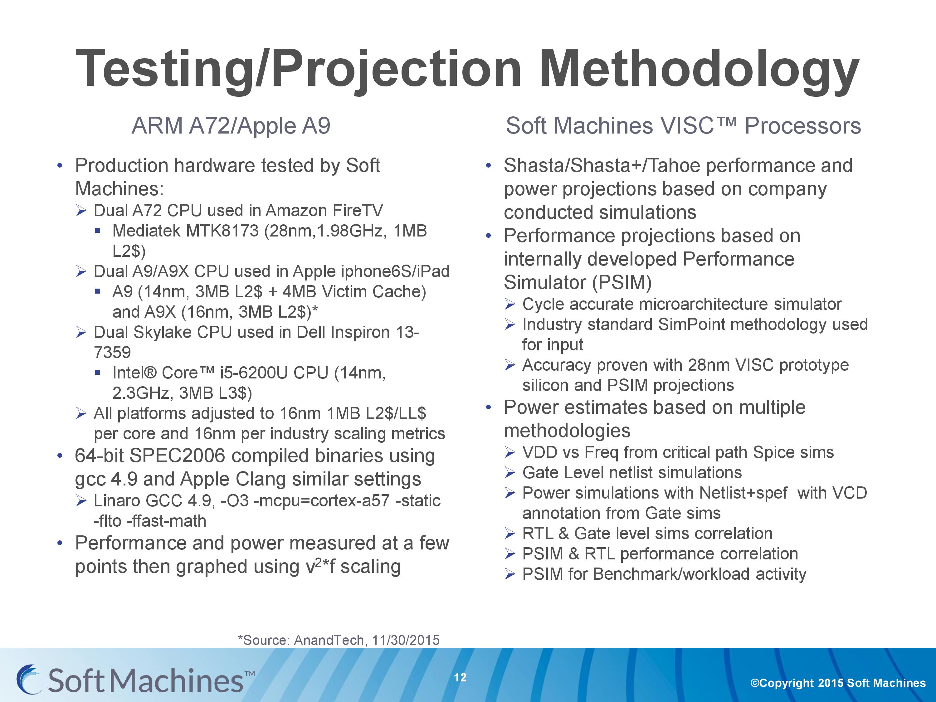
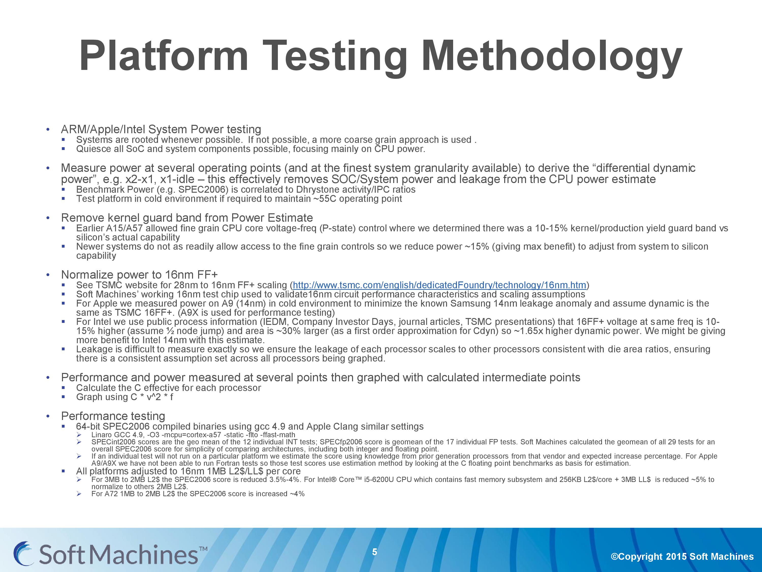
Because we were one of the last media outlets to speak with Soft Machines, and I had already seen some discussion around these points, I posed the issues back to them, as well as a few questions of my own. Because of the response that had been presented, we managed to get a lot of details around the simulation and assumptions aspects. So to start, here’s the testing methodology that everyone was provided with:
For clarity on the VISC processors, simulations were done to be both signal accurate and cycle accurate, and data taken from 16nm design configurations. Both power and results were taken from these.
For the power on the other parts, the power consumption was taken at the wall. To remove system power from the equation, the system was run in 2C vs 1C modes and 1C vs idle modes at various frequencies to find the dynamic power. Each platform was tested in a cold environment to ensure the maximum temperature did not go above 55C. Each of the power numbers are estimates that have removed the production yield ‘guard’ (i.e. protection overestimate), which was about ~15%, giving benefits to the non-VISC core results.
For the power conversion to 16nm FinFET+ on TSMC:
- The A72 28nm TSMC used TSMC’s numbers for scaling.
- For the A9X numbers, the A9 numbers were taken in a cool environment to minimize Samsung 14nm leakage and the dynamic power for the A9X is assumed the same as the A9.
- For Intel, using public data it was assumed that 16FF+ voltage is 10-15% higher and area is 30% larger, giving ~1.65x power on 16FF+.
- Leakage scales with die area.
For performance testing:
- Linaro GCC 4.9 with -O3 -mcpu=cortex-a57 -static -flto -ffast-math
- If any test failed, results were taken from previous generations and expected percentage increases. For example, FORTRAN on A9 failed, so estimates were taken from the floating point numbers in C.
- For the cache adjustments, for 3MB to 2MB was reduced 3.5-4%. Because Intel has L2+L3, this is reduced a further 5%. For A72 moving from 1MB L2 to 2MB L2 in total, score was increased by 4%.
For a full rundown, this was the slide provided to us:
As part of these assumptions, I did ask about the raw data collected and if that would ever be presented. I did mention that they really need to split up INT and FP results, and I was told that it may happen at a later date but not right now. What I was given though was the effect of the cache adjustment on Skylake.
The orange line and the blue line next to it represents the movement from a multi-cache hierarchy of L2+L3 to 1MB of L2 cache per core only. The blue line still has the assumption of moving from 14nm to 16FF+, and using the GCC compiler, but the orange line has that extra assumpton.
Personally, these assumptions make me uneasy. Conversions like this are typically only done as back-of-the-envelope types of calculations during the early stages of design, because they are very rough and do not take into account things like silicon floor-plan optimization that would occur if you chose a smaller/larger cache arrangement, or changing from 8-way to 4-way associativity in the caches and so on. Typically we see companies in similar positions to SMI provide the raw or semi-modified data, using one assumption at most, with a split between FP and INT results - e.g. taking all the results as-is with GCC. The reason why it all comes into one graph is for brief simplicity, which doesn't particularly endear any reader/investor who might decide to be heavily invested in this project.
We pointed out a lot of concerns with this data to Soft Machines, including the list above of assumptions and how some of them simply do not make sense and should be restricted to that those quick rough calculations, especially when presenting at a conference. They gave us the graph above showing the effect of cache changes on Skylake, but I have asked in the future for them to display the data in a less complicated way, using standard industry metrics (such as INT or FP). Ideally the graphs are also kept to two or three data sets without requiring a 9-point interpretation scheme to understand what is happening - we typically get a dozen or so graphs from Huawei, ARM, AMD or Intel when they are describing their latest architecture or microarchitecture designs. This allows more understanding of what is happening under the hood and can be used to validate the results - as it stands, it is difficult to validate anything due to the assumptions and conversions made.
But 16FF+ Silicon Exists
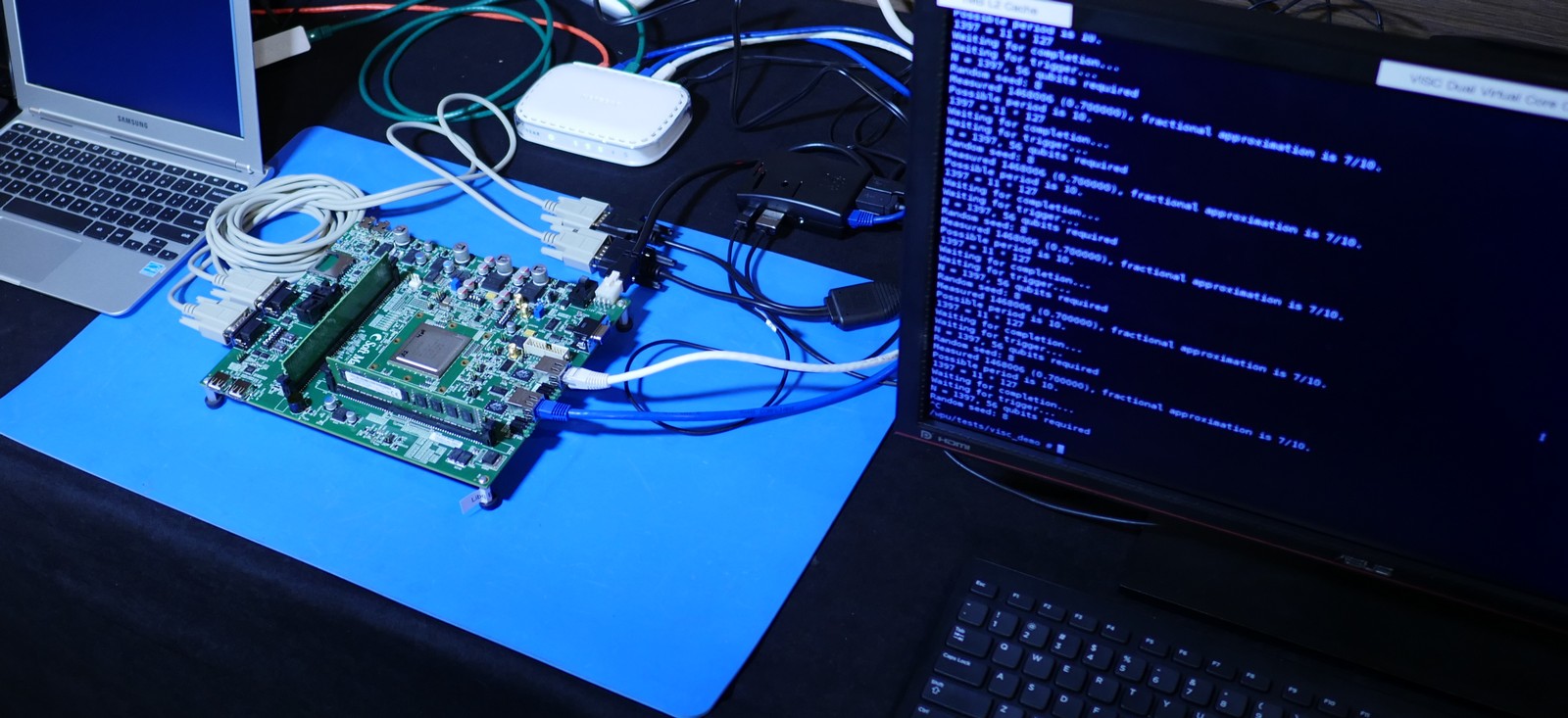
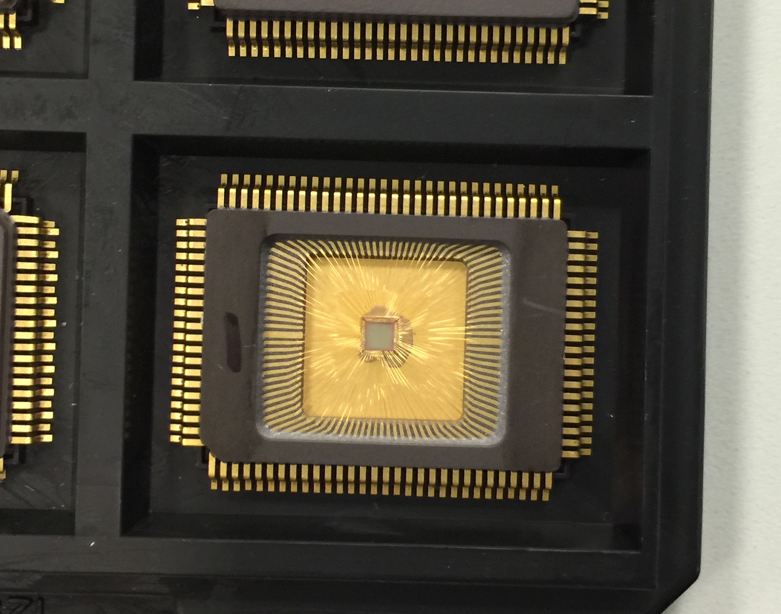
One of the salient points of our talk with Soft Machines was the fact that silicon talks louder than simulations. Their CTO was very honest and said this before I even had the chance to. The 28nm design was shown in 2014 and data was provided, but no 16FF+ design had since been made public. Soft Machines were happy enough to share with us that they do have the core design for 16nm at HQ being examined:
16nm Silicon of a Shasta design
This is literally a test chip of cores rather than a full SoC, and they are currently running the correlation data between simulation and silicon. We were told that the design errors that the 28nm silicon had, such as cache flushing properly, were fixed. The new silicon also includes power plane management, although customers are welcome to use their own power plane adjustments.
The goal, according to Soft Machines' numbers, is to provide a Shasta core on an optimized 16nm FF+ process at 2GHz at around 2W. Their goal includes scaling the design from SoC to server, meaning that there is the goal to reach a range of 0.5W per core up to 5W per core. Because there’s only one 16FF+ part-SoC early run currently at their headquarters it remains to be seen if that is possible, and requires a partner or investor to get their hands dirty with the technology first.
Before someone jumps up and says "is platform XYZ going to use VISC?", it should be fairly obvious from most public roadmaps covering the next 1-2 years that major platforms will not be using VISC. What we see on public roadmaps is a mix of ARM and x86, and the fact that VISC is a different ISA under the hood (which can run native VISC code without translation) means that there has to be an ecosystem change. Soft Machines, with their announcement last week, is at this time principally fishing for clients, investors, and potentially something more.
The big thing about why this design has got a lot of attention in the media and between analysts is because of the potential. Being able to have many light-weight cores that can share resources between threads would be a major milestone in semiconductor design and the next point in the CISC/RISC lineage. It epitomizes the idea of having all the hardware working on a task no matter what it is, such that you can have many slower power efficient cores working on a single task or one inefficient high power but fast core. If you can spare the die area and have a good ISA translation layer, this opens up some of the power budget in a power limited device. A lot of discussion on laptops or smartphones is all about the power, although Soft Machines believes this can impact servers just as easily.
Arguably one could state that future processors will have to do something like VISC in order to get better IPC – when a thread needs a large wide core, then a VISC design can be one when needed. Technically we already have semiconductor designs that work very well on prepared data – vector calculations and graphics are handled by lots of small, simple cores in their thousands. But these only work with consistent data and when the same calculation on all the data points is needed; with a VISC design, the code can be complex with dependencies and the virtual cores will shrink/expand as needed. A lot of questions surrounding the translation layer are to be expected, and if it can be as water-tight as possible when other ISAs are passed through (ARM to VISC, x86 to VISC) and also take advantage of compiler benefits as to SMI’s claims.
As it stands the design promises a lot, but because we really need to see the proper silicon implementation, it might be hard to visualize until a company in the technology ecosystem decides to make that step. It would be an interesting differentiation point for sure, but it requires investment to reach utility in mass production. That makes a number of analysts wary and conservative with good reasons, especially with the assumptions made on that data graph.
Soft Machines has invited us to their offices next time I’m in the Bay Area, which I will probably take them up on.
Sources:
Soft Machines
Microprocessor Report
2014 Linley Conference Video
2015 Linley Conference Video

