AMD Zen 3 Ryzen Deep Dive Review: 5950X, 5900X, 5800X and 5600X Tested
by Dr. Ian Cutress on November 5, 2020 9:01 AM ESTSection by Andrei Frumusanu
The New Zen 3 Core: High-Level
As we dive into the Zen3 microarchitecture, AMD made a note of their journey of the last couple of years, a success-story that’s been started off in 2017 with the revolutionary Zen architecture that helped bring AMD back to the competitive landscape after several sombre years of ailing products.
The original Zen architecture brought a massive 52% IPC uplift thanks to a new clean-sheet microarchitecture which brought at lot of new features to the table for AMD, introducing features such as a µOP cache and SMT for the first time into the company’s designs, as well as introducing the notion of CPU core-complexes with large (8MB at the time) L3 caches. Features on a 14nm FinFET process node, it was the culmination and the start-off point of a new roadmap of microarchitectures which leads into today’s Zen3 design.
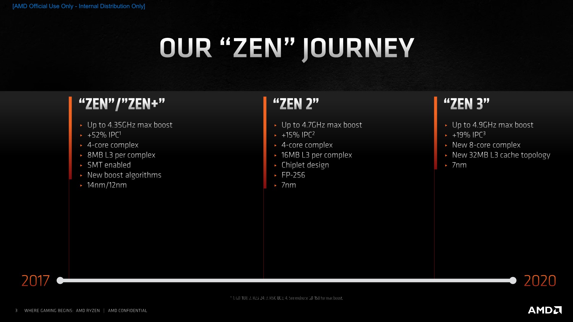
Following a minor refresh in the form of Zen+, last year’s 2019 Zen2 microarchitecture was deployed into the Ryzen 3000 products, which furthered AMD’s success in the competitive landscape. Zen2 was what AMD calls a derivative of the original Zen designs, however it contained historically more changes than what you’d expect from such a design, bringing more IPC increases than what you’d typically see. AMD saw Zen2 as a follow-up to what they had learned with the original Zen microarchitecture, fixing and rolling out design goal changes that they had initially intended for the first design, but weren’t able to deploy in time for the planned product launch window. AMD also stated that it enabled an opportunity to bring some of the future Zen3 specific changes were moved forward into the Zen2 design.
This was also the point at which AMD moved to the new chiplet design, leveraging the transition to TSMC’s new 7nm process node to increase the transistor budget for things like doubling the L3 cache size, increasing clock speeds, and vastly reducing the power consumption of the product to enable aggressive ramp in total core counts both in the consumer space (16-core Ryzen 9 3950X), as well as in the enterprise space (64-core EPYC2 Rome).
Tying a cutting-edge high-performance 7nm core-complex-die (CCD) with a lower cost 12/14nm I/O die (IOD) in such a heterogenous package allowed AMD to maximise the advantages and minimise the disadvantages of both respective technologies – all whilst AMD’s main competitor, Intel, was, and still is, struggling to bring out 10nm products to the market. It was a technological gamble that AMD many times has said was made years in advance, and has since paid off plenty.
Zen 3 At A Glance
This brings us to today’s Zen3 microarchitecture and the new Ryzen 5000 series. As noted earlier, Mark Papermaster had mentioned that if you were to actually look at the new design from a 100,000-foot level, you’d notice that it does look extremely similar to previous generation Zen microarchitectures. In truth, while Zen3 does share similarities to its predecessors, AMD’s architects started off with a clean-sheet design, or as they call it – “a ground-up redesign”. This is actually quite a large claim as this is a quite enormous endeavour to venture in for any company. Arm’s Cortex-A76 is the most recent other industry design that is said to have been designed from scratch, leveraging years of learning of the different design teams and solving inherent issues that require more invasive and large changes to the design.
Because the new Zen3 core still exhibits quite a few defining characteristics of the previous generation designs, I think that AMD’s take on a “complete redesign” is more akin to a deconstruction and reconstruction of the core’s building blocks, much like you’d dismantle a LEGO set and rebuild it anew. In this case, Zen3 seems to be a set-piece both with new building blocks, but also leveraging set pieces and RTL that they’ve used before in Zen2.
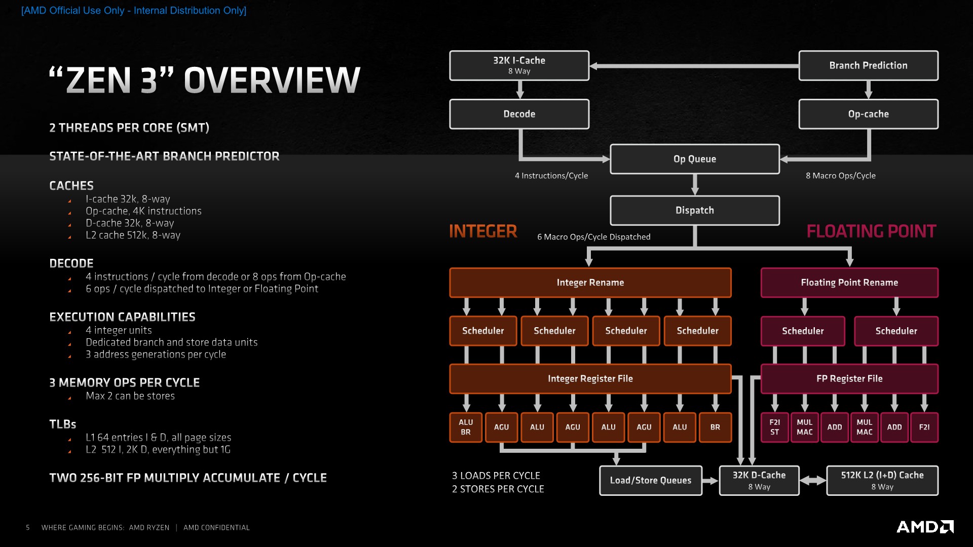
Whatever the interpretation of a “clean-sheet” or “complete redesign” might be, the important take is that Zen3 is a major overhaul in terms of its complete microarchitecture, with AMD paying attention to every piece of the puzzle and trying to bring balance to the whole resulting end-design, which comes in contrast to a more traditional “derivative design” which might only touch and see changes in a couple of the microarchitecture’s building blocks.

AMD’s main design goals for Zen3 hovered around three main points:
- Delivering another significant generational single-threaded performance increase. AMD did not want to be relegated to top performance only in scenarios where workloads would be spread across all the cores. The company wanted to catch up and be an undisputed leader in this area to be able to claim an uncontested position in the market.
- Latency improvements, both in terms of memory latency, achieved through a reduction in effective memory latency through more cache-hits thanks to the doubled 32MB L3 that an individual core can take advantage of, as well as core-to-core latency which again thanks to the consolidated single L3 cache on the die is able to reduce long travel times across the dies.
- Continuing a power efficiency leadership: Although the new Zen3 cores still use the same base N7 process node from TSMC (although with incremental design improvements), AMD had a constraint of not increasing power consumption for the platform. This means that any new performance increases would have to come through simultaneous power efficiency improvements of the microarchitecture.
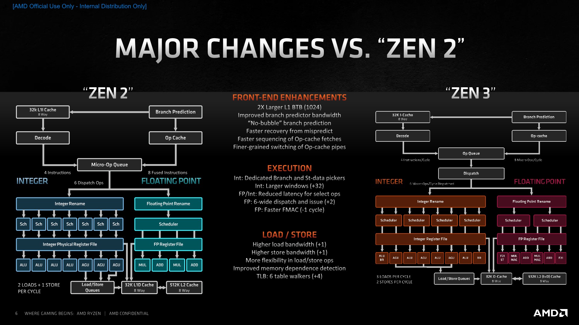
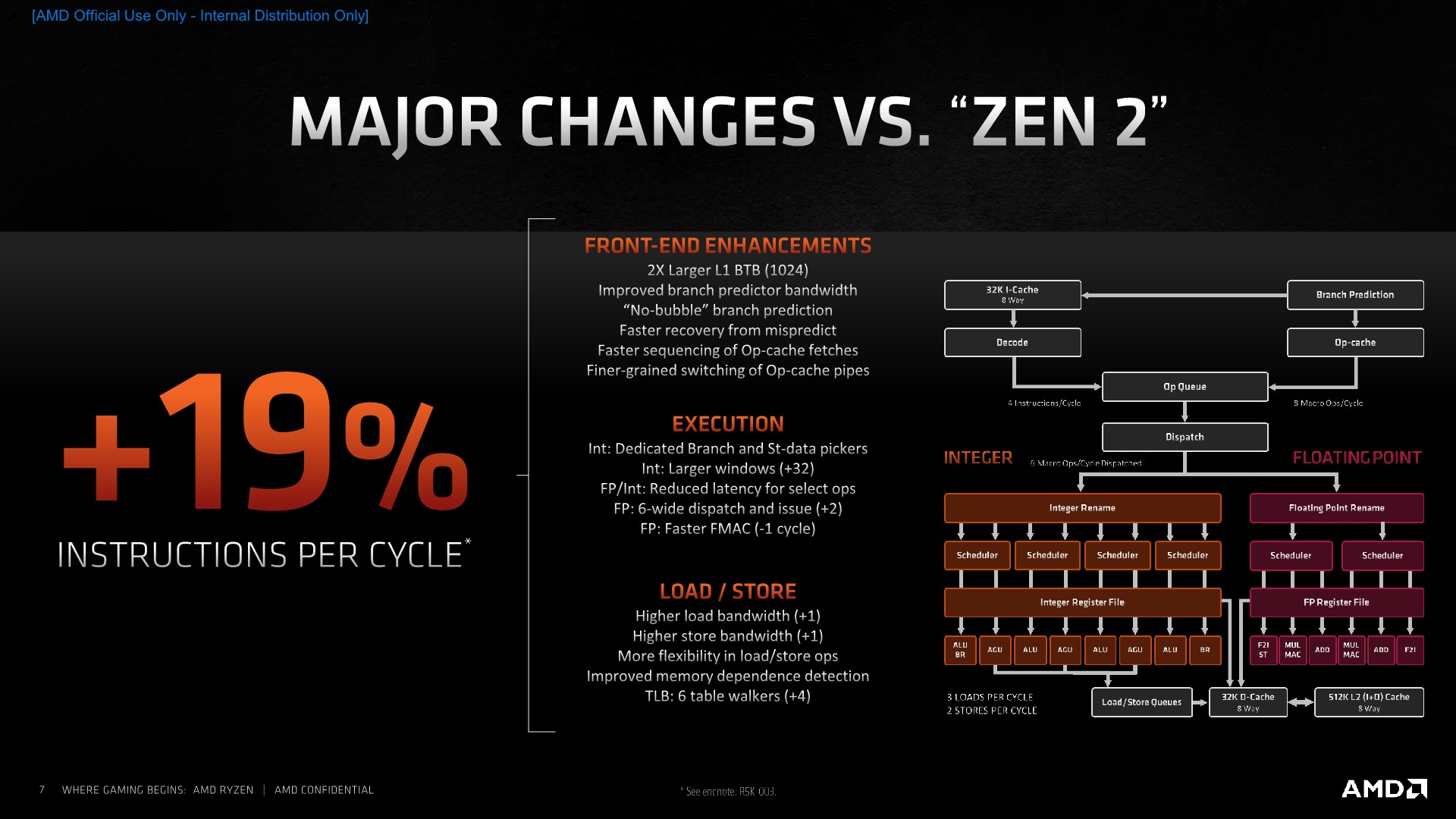
The culmination of all the design changes AMD has made with the Zen3 micro-architecture results in what the company claims as a 19% average performance uplift over a variety of workloads. We’ll be breaking down this number further into the review, but internal figures show we are matching the 19% average uplift across all SPEC workloads, with a median figure of 21%. That is indeed a tremendous achievement, considering the fact that the new Ryzen 5000 chips clock slightly higher than their predecessors, further amplifying the total performance increase of the new design.


339 Comments
View All Comments
Orkiton - Thursday, November 5, 2020 - link
Please Anandtech, up ryzen and up epic your servers, it's ages here to load a page...PrionDX - Thursday, November 5, 2020 - link
Mmm nice warm code bath, very relaxing> Results for Cinebench R20 are not comparable to R15 or older, because both the scene being used is different, but also the updates in the code bath.
prophet001 - Thursday, November 5, 2020 - link
How you gonna test FFXIV and not WoW.-______________-
Mr Perfect - Thursday, November 5, 2020 - link
Guys, could you please define acronyms the first time they are used in an article? Take page three for example, it touches on a BTB, TAGE and ITA, but only ITA is defined. I have no idea what a BTB or TAGE is. If they where defined on page two and I missed them, feel free to ignore me.name99 - Saturday, November 7, 2020 - link
BTB= Branch Target Buffer. Holds the addresses where a branch will go if it taken.TAGE= (tagged geometric something-or-other) name is not important; what matters is that it's currently the most accurate known branch predictor. Comes in a few variants, was 1st published around 2007 by Andre Seznec who has since gone on to show how it can be used for damn well everything! (Value prediction, indirect branch, prefetching, washing windows, you name it.)
Apple seems to have been first to implement, maybe as early as the A7, certainly very soon in the A series.
Now everybody uses it, but only in the last year or so has everyone really got on board. (Actually to be precise Seznec suggested that Intel is using TAGE based on their performance characteristics, but I don't think Intel have confirmed this. And ARM probably are but again unconfirmed. IBM is confirmed, and now AMD.)
Even if you know the basic algorithm for direction prediction is TAGE, that still doesn't make everyone equal. There are MANY extra aspects where everyone is different. The most obvious is how much storage is given to the branch predictor, but other less obvious aspects include
- how do you predict indirect branches? State of the art is ITTAGE, but that doesn't mean everyone is using it.
- how do you update your branch prediction storage (ie how fast do corrections get from the backend into the predicting mechanism at the front end)
- how do you implement your L2 storage and second-stage prediction?
- what extra "specialist" predictors do you have? (These are things like special-case predictors for loops.)
quantcon - Thursday, November 5, 2020 - link
Yeah, it's actually kinda nuts, considering Intel convinced us years ago that we've hit the point of diminishing returns and there are hardly any IPC improvements to be had.Spunjji - Sunday, November 8, 2020 - link
Seems like they needed to believe that...DanD85 - Thursday, November 5, 2020 - link
This just goes on to prove yet again how crucial a healthy competition benefits everyone. Intel has been stagnating for more than a decade. Imagine where we would have been performance-wise if we had got this ~40% increase every 3 years. Intel only have themselves to blame. They are the chipzillla, the gatekeeper and the choker of the whole industry!lmcd - Monday, November 9, 2020 - link
40% is a bit disingenuous. Most of the gap in desktop is chiplet design. Notice how mobile, while AMD-favored, is still competitive? It's just a bad bet from Intel going with stacked packaging before same-package flat chiplet, and the packaging techniques for both are very new. There aren't 40% improvements on the table going forward, Bulldozer and Piledriver were both just awful and AMD didn't ever release full desktop Steamroller or Excavator (which were fine, not great). Zen 1 left a lot on the table for such a big increase as well.GeoffreyA - Tuesday, November 10, 2020 - link
If you place Zen at Haswell's level, it took AMD three years to reach Zen 3 (from the consumer's point of view). On Intel's side, it's taken six years to go from Haswell to Sunny Cove.Even in the early tick-tock days, when more massive changes could be put in, it was usually two years apart for microarchitecture: Core (2006), Nehalem (2008), Sandy Bridge (2010/11), etc.
Whether there's a lot more juice in the tank for Zen remains to be seen. In my opinion I think there is: Z3's out-of-order structures are still quite conservative, compared to Sunny Cove, which it beats, so there's possibility of more widening there. I also think their split scheduler design, inherited from the Athlon, will allow them to scale more easily. Of course, I know the engineers in Haifa must be cooking up something potent too. Either way, exciting stuff.