NVIDIA Announces PCIe A100 Accelerator: 250 Watt Ampere In A Standard Form Factor
by Ryan Smith on June 22, 2020 3:30 AM EST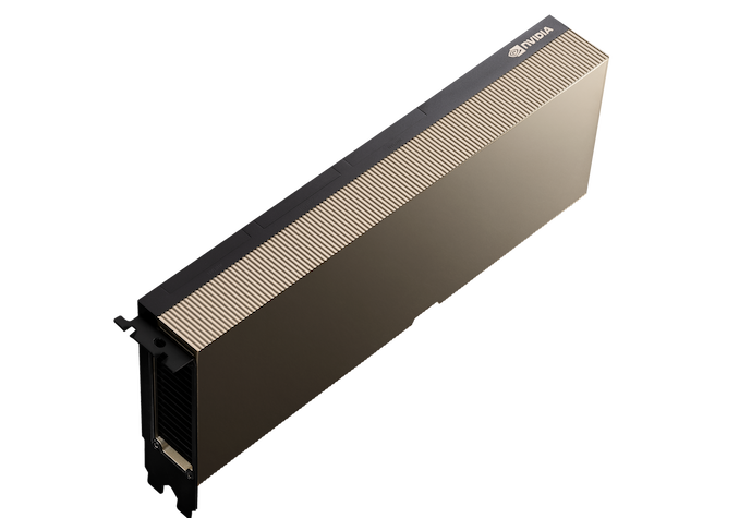
With the launch of their Ampere architecture and new A100 accelerator barely a month behind them, NVIDIA this morning is announcing the PCIe version of their accelerator as part of the start of the now-virtual ISC Digital conference for high performance computing. The more straight-laced counterpart to NVIDIA’s flagship SXM4 version of the A100 accelerator, the PCie version of the A100 is designed to offer A100 in a more traditional form factor for customers who need something that they can plug into standardized servers. Overall the PCIe A100 offers the same peak performance as the SXM4 A100, however with a lower 250 Watt TDP, real-world performance won’t be quite as high.
The obligatory counterpart to NVIDIA’s SXM form factor accelerators, NVIDIA’s PCIe accelerators serve to flesh out the other side of NVIDIA’s accelerator lineup. While NVIDIA would gladly sell everyone SXM-based accelerators – which would include the pricey NVIDIA HGX carrier board – there are still numerous customers who need to be able to use GPU accelerators in standard, PCIe-based rackmount servers. Or for smaller workloads, customers don’t need the kind of 4-way and higher scalability offered by SXM-form factor accelerators. So with their PCIe cards, NVIDIA can serve the rest of the accelerator market that their SXM products can’t reach.
The PCIe A100, in turn, is a full-fledged A100, just in a different form factor and with a more appropriate TDP. In terms of peak performance, the PCIe A100 is just as fast as its SXM4 counterpart; NVIDIA this time isn’t shipping this as a cut-down configuration with lower clockspeeds or fewer functional blocks than the flagship SXM4 version. As a result the PCIe card brings everything A100 offers to the table, with the same heavy focus on tensor operations, including the new higher precision TF32 and FP64 formats, as well as even faster integer inference.
| NVIDIA Accelerator Specification Comparison | ||||||
| A100 (PCIe) |
A100 (SXM4) |
V100 (PCIe) |
P100 (PCIe) |
|||
| FP32 CUDA Cores | 6912 | 6912 | 5120 | 3584 | ||
| Boost Clock | 1.41GHz | 1.41GHz | 1.38GHz | 1.3GHz | ||
| Memory Clock | 2.43Gbps HBM2 | 2.43Gbps HBM2 | 1.75Gbps HBM2 | 1.4Gbps HBM2 | ||
| Memory Bus Width | 5120-bit | 5120-bit | 4096-bit | 4096-bit | ||
| Memory Bandwidth | 1.6TB/sec (1555GB/sec) |
1.6TB/sec (1555GB/sec) |
900GB/sec | 720GB/sec | ||
| VRAM | 40GB | 40GB | 16GB/32GB | 16GB | ||
| Single Precision | 19.5 TFLOPs | 19.5 TFLOPs | 14.1 TFLOPs | 9.3 TFLOPs | ||
| Double Precision | 9.7 TFLOPs (1/2 FP32 rate) |
9.7 TFLOPs (1/2 FP32 rate) |
7 TFLOPs (1/2 FP32 rate) |
4.7 TFLOPs (1/2 FP32 rate) |
||
| INT8 Tensor | 624 TOPs | 624 TOPs | N/A | N/A | ||
| FP16 Tensor | 312 TFLOPs | 312 TFLOPs | 112 TFLOPs | N/A | ||
| TF32 Tensor | 156 TFLOPs | 156 TFLOPs | N/A | N/A | ||
| Relative Performance (SXM Version) | 90% | 100% | N/A | N/A | ||
| Interconnect | NVLink 3 12 Links (600GB/sec) |
NVLink 3 12 Links (600GB/sec) |
NVLink 2 4 Links (200GB/sec) |
NVLink 1 4 Links (160GB/sec) |
||
| GPU | GA100 (826mm2) |
GA100 (826mm2) |
GV100 (815mm2) |
GP100 (610mm2) |
||
| Transistor Count | 54.2B | 54.2B | 21.1B | 15.3B | ||
| TDP | 250W | 400W | 250W | 300W | ||
| Manufacturing Process | TSMC 7N | TSMC 7N | TSMC 12nm FFN | TSMC 16nm FinFET | ||
| Interface | PCIe 4.0 | SXM4 | PCIe 3.0 | SXM | ||
| Architecture | Ampere | Ampere | Volta | Pascal | ||
But because the dual-slot add-in card form factor is designed for lower TDP products, offering less room for cooling and typically less access to power as well, the PCIe version of the A100 does have to ratchet down its TDP from 400W to 250W. That’s a sizable 38% reduction in power consumption, and as a result the PCIe A100 isn’t going to be able to match the sustained performance figures of its SXM4 counterpart – that’s the advantage of going with a form factor with higher power and cooling budgets. All told, the PCIe version of the A100 should deliver about 90% of the performance of the SXM4 version on single-GPU workloads, which for such a big drop in TDP, is not a bad trade-off.
And on this note, I should give NVIDIA credit where credit is due: unlike the PCIe version of the V100 accelerator, NVIDIA is doing a much better job of documenting these performance differences. This time around NVIDIA is explicitly noting the 90% figure in their their specification sheets and related marketing materials. So there should be a lot less confusion about how the PCIe version of the accelerator compares to the SXM version.

Other than the form factor and TDP changes, the only other notable deviation for the PCIe A100 from the SXM version is how NVLink connections work. For their PCIe card NVIDIA is once again using NVLink bridges connected across the top of A100 cards, allowing for two (and only two) cards to be linked together. The upshot is that with 3 NVLink connectors, all 12 of the GA100's GPU physical links are being exposed, meaning that the card has full access to its NVLink bandwidth. So although you can only talk to one other PCIe A100 card, you can do so at a speedy 300GB/sec in each direction, 3x the rate a pair of V100 PCIe cards communicated at.
Otherwise the PCIe A100 comes with the usual trimmings of the form factor. The card is entirely passively cooled, designed to be used with servers with powerful chassis fans. And though not pictured in NVIDIA’s official shots, there are sockets for PCIe power connectors. Meanwhile, with the reduced usage of NVLink in this version of the card, A100’s native PCIe 4 support will undoubtedly be of increased importance here, underscoring the advantage that an AMD Epyc + NVIDIA A100 pairing has right now since AMD is the only x86 server vendor with PCIe 4 support.
Wrapping things up, while NVIDIA isn’t announcing specific pricing or availability information today, the new PCIe A100 cards should be shipping soon. The wider compatibility of the PCIe card has helped NVIDIA to line up over 50 server wins at this point, with 30 of those servers set to ship this summer.
Source: NVIDIA


29 Comments
View All Comments
mode_13h - Wednesday, June 24, 2020 - link
Thanks. I was looking for that, as well, but didn't find any such specs.eddman - Monday, June 22, 2020 - link
Are you sure the GPU chip is also called A100? Even nvidia calls it GA100:https://devblogs.nvidia.com/nvidia-ampere-architec...
I think the confusion arises from the fact that they refer to their tensor accelerator products as "GPU"; e.g. "NVIDIA V100 TENSOR CORE GPU", "NVIDIA A100 Tensor Core GPU".
In other words, when they say "A100 GPU", they mean the card, not the actual GPU chip.
eddman - Monday, June 22, 2020 - link
https://www.nvidia.com/content/dam/en-zz/Solutions...Page 37
Ryan Smith - Monday, June 22, 2020 - link
Ahh yep, there's a typo. Thanks!eddman - Monday, June 22, 2020 - link
The same error was made in your first ampere/A100 article:"Officially, this is the name of both the GPU and the accelerator incorporating it; and at least for the moment they’re both one in the same, since there is only the single accelerator using the GPU."
CiccioB - Monday, June 22, 2020 - link
The same mistake was done with Volta launch, where the V100 accelerator name was commonly exchanged with GV100 when talking about the GPU by itself.jeremyshaw - Monday, June 22, 2020 - link
So, is most of the power reduction actually coming from cutting the NVLinks down? I don't know about the current NVLink, but the first two versions, Nvidia claimed they didn't have to do external retimers or redrivers, which I can only assume drove up the power consumption, especially with the distances some of the NVLink signals have to travel on the HGX/DGX system vs a NVLink bridge.eastcoast_pete - Monday, June 22, 2020 - link
Thanks Ryan! Also, just to add that cold shower that reality provides so well, I suggest to add the MSRP for those cards. Yes, they'll all run Crysis, but... (And the accelerators don't even have a video signal out)mode_13h - Tuesday, June 23, 2020 - link
Did they even announce a list price? I don't see it in the press release.I'm betting the street price will be in excess of $10k.