Chipworks Provides First Apple A7 Die Shot
by Anand Lal Shimpi on September 20, 2013 5:57 PM EST- Posted in
- Smartphones
- Apple
- Mobile
- SoCs
- iPhone 5S
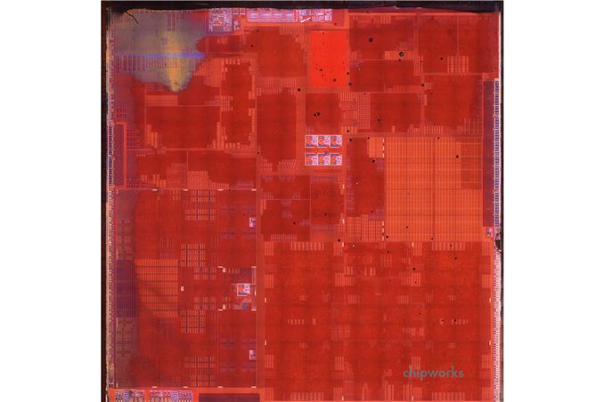
Hot on the heels of their Samsung 28nm confirmation, Chipworks just sent over the first die shot of a delayered Apple A7. An annotated version is following early next week, but I've highlighted two sections of interest:
In yellow we have what appears to be the two Cyclone CPU cores. If those are indeed the two CPU cores, the layout does seem different than what we saw last year with Swift in the A6. Also note that the percentage of die area dedicated to the CPU appears to have grown a small amount (now roughly 17% of the total SoC area).
To the lower right I found four replicated blocks with some shared logic in between (highlighted in light blue). I'm wondering if this area isn't the 4-cluster PowerVR G6430 from IMG. All of this is just a quick educated guess of course.
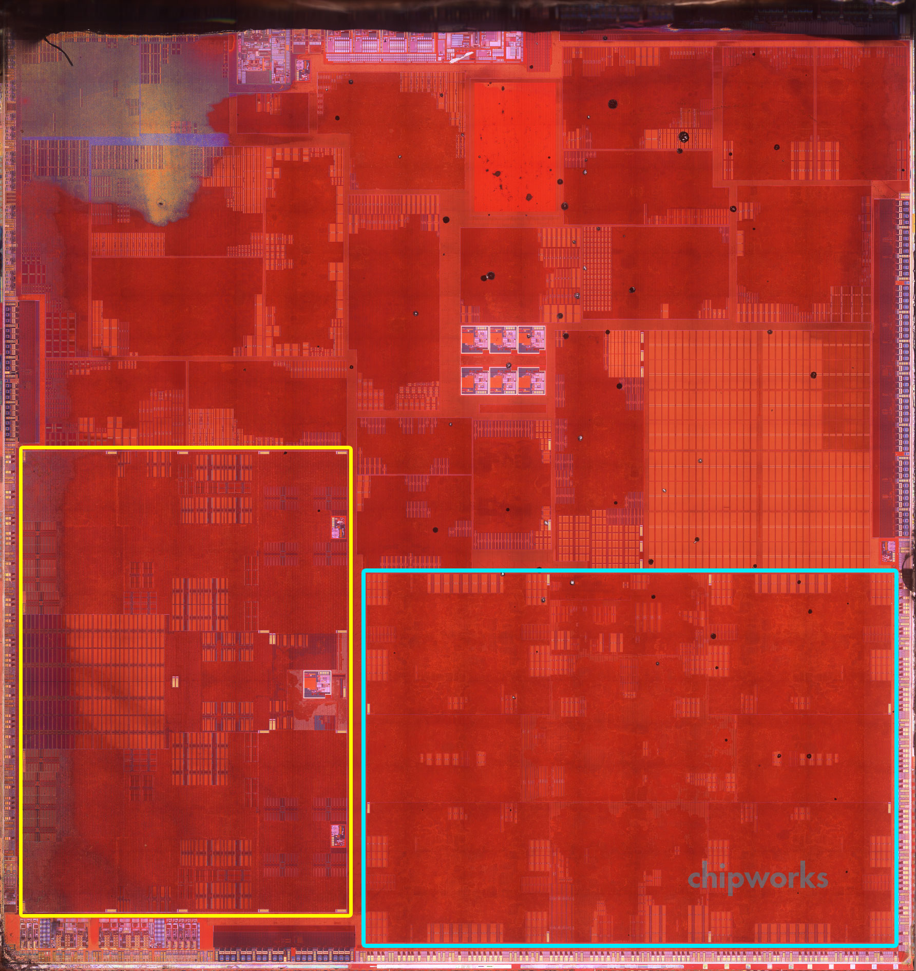 Apple A7, Photo from Chipworks, annotations mine
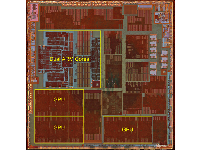 Apple A6, Photo & Annotations from Chipworks
Apple has already confirmed die size (102mm^2) and roughly confirmed transistor count (over 1B) of the A7 so everything else is mostly a known quantity at this point.
| Apple A7 vs A6 SoCs | ||||
| Apple A7 (2013) | Apple A6 (2012) | |||
| Manufacturing Process | Samsung 28nm HKMG | Samsung 32nm HKMG | ||
| Die Size | 102mm2 | 97mm2 | ||
| Transistor Count | "Over 1B" | ? | ||
| CPU | 2 x Apple Cyclone ARMv8 64-bit cores | 2 x Apple Swift ARMv7 32-bit cores | ||
| GPU | IMG PowerVR G6430 | IMG PowerVR SGX 543MP3 | ||
Source: Chipworks


39 Comments
View All Comments
stacey94 - Saturday, September 21, 2013 - link
Because it says that it's an NXP LPC1800.Apple got it off the shelf from these guys and labeled it the M7:
http://www.nxp.com/products/microcontrollers/corte...
bhd2 - Monday, September 23, 2013 - link
Hi,We (at Chipworks) did some poking around on the NXP website, looking at their LPC range of products; and we couldn't find any specific part that matched the look of the LPC18A1, particularly the 30-ball WLCSP packaging. So we've come to the tentative conclusion that this is likely a customised LPC18xx chip built for Apple, similar to those we've seen from Dialog and Cirrus over the years (A1 stands for Apple-1?).
Could be M3, could be M0 (though the latter don't have the LPC18 prefix).
toyotabedzrock - Tuesday, September 24, 2013 - link
If it was truly custom it would have been printed with an apple logo. They just ordered a specific package.dylan522p - Saturday, September 21, 2013 - link
When the review was originally posted Anand had not completely figured it all out yet and said that Oscar was the CPU and had no mention of Cyclone. He later fixed it.name99 - Friday, September 20, 2013 - link
What's with the obviously differently colored parts that look higher res?We see a block of six of them in the middle of the chip, a seventh one in the CPU part, and two smaller versions also in the CPU part.
Are those real or some image processing artifact of Chipworks and/or Anand trying to modify those parts of the image for higher contrast and sharpness?
Tom Womack - Saturday, September 21, 2013 - link
I think they're probably clock generators (PLLs)bhd2 - Saturday, September 21, 2013 - link
They are not a processing artefact, it would be really difficult to select those areas for special treatment - it appears to be the effect of different device density. At this points I think PLLs is a good guess; if you look at the A6 image there are similar blocks in the top-left quadrant.bartoni - Saturday, September 21, 2013 - link
Yes, the six small identical square blocks in the middle and the one square between the cores are very likely PLLs.tipoo - Saturday, September 21, 2013 - link
It's because of different layouts and densities. It's the same reason you get different colors within the same decapped chip.HisDivineOrder - Saturday, September 21, 2013 - link
Can't wait to see the iPad based on this SOC.