AMD Radeon HD 7790 Review Feat. Sapphire: The First Desktop Sea Islands
by Ryan Smith on March 22, 2013 12:01 AM EST- Posted in
- GPUs
- AMD
- Sapphire
- GCN
- Radeon HD 7000
Bonaire’s Microarchitecture - What We’re Calling GCN 1.1
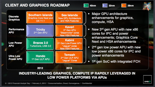
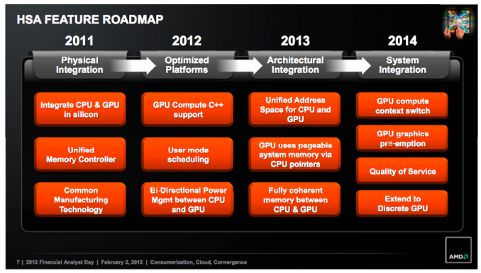
With our introduction out of the way, before looking at the cards and our performance results we would like to dive into a technical discussion and a bit of nitpicking. Specifically we would like to spend some time talking about architectures and product naming, as it’s going to be a bit confusing at first. As AMD has stated numerous times in the past, Graphics Core Next is a long-term architecture for the company. AMD intends to evolve GCN over the years, releasing multiple microarchitectures based on GCN that improve the architecture and add features while still being rooted in the design principles of GCN. GCN is after all the other half of AMD’s upcoming HSA-capable APUs, the culmination of years of AMD’s efforts with HSA/Fusion.
So where does Bonaire fit in? Bonaire is of course a GCN part; it’s a new microarchitecture that’s technically different from Southern Islands, but on the whole it’s a microarchitecture that’s extremely close in design to Southern Islands. In this new microarchitecture there are some changes – among other things the new microarchitecture implements some new instructions that will be useful for HSA, support for a larger number of compute work queues (also good for HSA) and it also implements a new version of AMD’s PowerTune technology (which we’ll get to in a bit) – but otherwise the differences from Southern Islands are very few. There are no notable changes in shader/CU efficiency, ROP efficiency, graphics features, etc. Unless you’re writing compute code for AMD GPUs, from what we know about this microarchitecture it’s likely you’d never notice a difference.
Unfortunately AMD has chosen to more-or-less gloss over the microarchitectural differences altogether, which is not wholly surprising since they will be selling Bonaire and previous generation products side-by-side. Bonaire’s microarchitecture has no official name (at least not one AMD wants to give us) and no version number. The Sea Islands name we’ve been seeing thrown around is not the microarchitecture name. Sea Islands is in fact the name for all of the GPUs in this wave – or perhaps it would be better to say all of the products created in this development cycle – including both Bonaire and it’s new microarchitecture, and Oland, AMD’s other new GPU primarily for mobile that is purely Southern Islands in microarchitecture.

In fact if not for the fact that AMD released (and then retracted) an ISA document called “AMD Sea Islands Instruction Set Architecture” last month, we would likely know even less about Bonaire’s microarchitecture. The document has been retracted at least in part due to the name (since AMD will not be calling the microarchitecture Sea Islands after all), so as a whole AMD isn’t particularly keen in talking about their microarchitecture at this time. But at the same time from a product standpoint it gives you an idea of how AMD is intending to smoothly offer both Southern Islands and Bonaire microarchitecture parts together as one product family.
Anyhow, for the sake of our sanity and for our discussions, in lieu of an official name from AMD we’re going to be retroactively renaming AMD’s GCN microarchitectures in order to quickly tell them apart. For the rest of this article and in future articles we will be referring to Southern Islands as GCN 1.0, while Bonaire’s microarchitecture will be GCN 1.1, to reflect the small changes between it and the first rendition of GCN.
Ultimately the differences between GCN 1.0 and GCN 1.1 are extremely minor, but they are real. But despite our general annoyance in how this has been handled, for consumers the difference between a GCN 1.0 card like the 7770 and a GCN 1.1 card like the 7790 should be limited to their innate performance differences, and of course PowerTune. GCN 1.1 or not, Bonaire fits in nicely in AMD’s current product stack and is in a position where it’s reasonable for it to be lumped together with GCN 1.0 parts as a single family. It’s really only the technical enthusiasts (like ourselves) and programmers that should have any significant reason to care about GCN 1.0 versus GCN 1.1. For everyone else this may just as well be another Southern Islands part.


107 Comments
View All Comments
GivMe1 - Friday, March 22, 2013 - link
128bit interface is going to hurt high res textures...CeriseCogburn - Sunday, March 24, 2013 - link
Oh no it won't ! this is amd man! nothing hurts when it's amd ! amd yes it can !Quizzical - Friday, March 22, 2013 - link
Your chart shows Radeon HD 6870 FP64 performance as N/A. I think it's 1/20 of FP32 performance, but I'm not sure of that. It definitely can do FP64, as otherwise, it wouldn't be able to claim OpenGL 4 compliance.MrSpadge - Friday, March 22, 2013 - link
No, it doesn't have any HARDWARE FP64 capabilities. It's always possible to emulate this at slow performance via software, though.Quizzical - Friday, March 22, 2013 - link
It's basically the same as what the 7770, 7790, and 7850 do, but they're not listed as N/A. The relevant question isn't whether you can do it more slowly, but how much more slowly.MrSpadge - Tuesday, March 26, 2013 - link
No, it's not the same, the GCN cards have hardware FP64 capabilities.Ryan Smith - Friday, March 22, 2013 - link
Let's be clear here. 85W is not the TDP. The TDP is higher (likely on the order of 110W or so). However AMD chooses not to publish the TDP for these lower end cards, and instead the TBP.alwayssts - Friday, March 22, 2013 - link
Yeah, I figure ~85 TBP/105w TDP because that would be smack between 7770/7850 as well as having 20% headroom (which also allows another product to have their TBP between there and 7850's max TDP with it's max tdp above it within 150w....ie ~120-125/150w). IIRC, 80w is the powertune max (TDP) of 7770, 130w for 7850. 85w is the stock operation (TBP) of 7790.I really, really dislike how convoluted this power game has become...can you tell?!
First it was max power. Then it was nvidia stating typical power (so products were within pci-e spec) with AMD still quoting max, which made them look bad. Then we get this 'awesome' product segmentation with 7000 having TBP and max powertune TDPs to separate them, while nvidia quotes TBP and hides the fact the TDP limits for their products exist unless you deduce them from the percentage you can up the boost power.
AAAAaaaarrrrrghhhhh. I miss when the product you had could do what you wanted it to, ie before software voltage control and multiple states, as for products like this it gives the user less control and the companies a ton to create segmentation. Low-end stock products may have been less-than-stellar back in the day, but with determination you could get something out of it without some marketing stating it should fit x niche so give it y max tdp so it doesn't interfere with the market of z product.
CeriseCogburn - Friday, March 22, 2013 - link
Maybe so you couldn't blow the crap out of it then return it for another one, then another one, as "you saved money" and caused everyone else to pay 25% more since you overclock freaks would blow them up, then LIE and get the freebie replacement, over and over again.Maybe they got sick of dealing with scam artist liars... maybe they aren't evil but the end user IS.
Spunjji - Friday, March 22, 2013 - link
Why would the design power be higher than the total board power? :/ You're correct that the figure they're quoting isn't TDP but then you just went and made up a number.Here's some actual power consumption measurements of a 7770:
http://www.techpowerup.com/reviews/HIS/HD_7770_iCo...
So using Ananad's figures to extrapolate you can expect this thing to be ~90W max, usually lower than that at peak, right about where AMD put it.