Welcome to Valhalla: Inside the New 250GB Xbox 360 Slim
by Anand Lal Shimpi on June 18, 2010 1:59 AM ESTI own a total of five Xbox 360s. Four of them have died. Three because of the Red Ring of Death, all out of warranty. Many have had serial Xbox 360 failures, I had them in parallel.
The last revision of the Xbox 360, codenamed Jasper, was supposed to fix the infamous RRoD problem. So far my Jasper has been running fine. While Microsoft never confirmed the cause the RRoD seemed to be a result of poor cooling and manufacturing issues (either at the die/underfill level or at the solder level or both).
Needless to say, I wasn’t terribly happy about purchasing a sixth Xbox 360, but here it is:
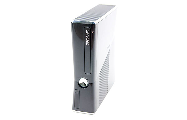
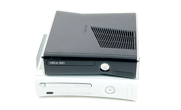
This is the latest revision of the Xbox 360, commonly referred to as the Xbox 360 Slim thanks to its shrinking in virtually all dimensions compared to the previous white box:
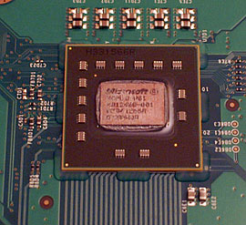
The internals are mostly new, featuring for the first time a single chip with CPU, GPU and eDRAM. Prior to this motherboard revision the Xbox 360 motherboard had two discrete packages, one with the CPU and one with the GPU + eDRAM.
 |
 |
For those of you who don't remember, ATI originally designed the Xbox 360's GPU and called it Xenos. The GPU was the first we ever looked at that used a unified shading architecture, so there were no dedicated pixel or vertex units. The core was made up of 48 shader processors and each SP could work on a vect4 plus a scalar op in parallel. These days we'd probably call it a GPU with 240 cores, although it's a bit dated from a functionality standpoint. The GPU runs at 500MHz and is also home to the memory controller.
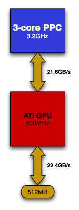
On a separate die, which ATI referred to as the daughter die, was 10MB of embedded DRAM along with all of the hardware necessary for z and stencil operations, color and alpha processing and AA. This eDRAM and associated logic helped Microsoft bring AA to games and improve overall performance compared to what was possible at the time with conventional architectures.
The CPU, codenamed Xenon, implemented three in-order PowerPC cores with SMT support - meaning the whole chip could work on six threads at the same time. The design was ahead of its time but given its 90nm manufacturing process it only had 1MB of L2 cache to share among all three cores. These days it isn't really considered the ideal approach to a many-core CPU. Private L2 caches with a large shared L3 cache is preferred for scaling beyond two cores.
Leading up to Jasper, each die was shrunk independently with each Xbox iteration. The table below shows us how:
| Xbox 360 Revision | CPU | GPU | eDRAM |
| Xenon/Zephyr | 90nm | 90nm | 90nm |
| Falcon/Opus | 65nm | 80nm | 80nm |
| Jasper | 65nm | 65nm | 80nm |
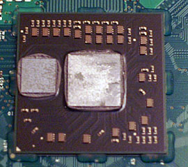
With the new Xbox 360 (codenamed Valhalla), at least two, possibly all three of the die are combined and placed on a single package:
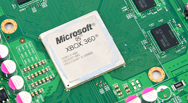
Bringing it all onto (presumably) a single die makes cooling much simpler as now there’s only one heatsink and one fan for all of the major heat generating components in the unit. This level of integration is made possible only by the not-so-magic of Moore’s Law. At 40nm it shouldn’t be a problem to bring all of those components onto a single reasonably sized die, which in turn reduces Microsoft’s manufacturing costs. It’s not totally clear whether Microsoft is building these chips on a 40nm, 45nm or 55nm node. The 40nm approach would make the most sense but TSMC is very capacity constrained at this point so it would be a slow ramp before all Xboxes got the Valhalla treatment. Update: Apparently 45nm is the magic number. The new CGPU is rumored to be made at Chartered Semiconductor, now under the ownership of Global Foundries.
The uncertainty is because of a pesky heat spreader. While previous Xbox 360 CPU/GPUs were visible to the naked eye once you popped the heatsink off, the Valhalla design has a heat spreader covering the Xbox CGPU (Microsoft’s term, not mine). Unwilling to potentially kill yet another Xbox 360, I’ve left my heat spreader intact for the purposes of this article.
What follows is an entire dissection guide for those of you who want to get inside the new Xbox 360 (for whatever reason you might have ;), as well as some power/noise information for those of you contemplating the upgrade.
Enjoy.


109 Comments
View All Comments
Visual - Friday, June 18, 2010 - link
does the wifi module work on a PC?does another type of wifi module that was ment for PCs work with the xbox?
are you able to open the hdd case and replace the hdd inside?
Ganesh_balan - Friday, June 18, 2010 - link
Anand,Could you please give us an insight into the fan details? Is that a Coolermaster make as it came out in the initial batch of leaked pics from the Chinese website? What size/rpm?
jigglywiggly - Friday, June 18, 2010 - link
Uhm, I am going to be the first to say this...It's hardly any smaller! (Not that the 360 is big)
Also it looks like a normal 360 and someone got a heatgun on the faceplate and it bent inwards.
michal1980 - Friday, June 18, 2010 - link
You need a special port for this add on?biohazard75 - Friday, June 18, 2010 - link
Yes and no. The Kinect connects to the 360 via a USB port, however it also requires more power than can be supplied by the USB port.So the 'new' Kinect port on the new 360 allows the Kinect to be connected via a single wire.
Connecting the Kinect to an old 360 requires an additional power lead (probably a power injected USB connector will be supplied).
(I never want to type Kinect/Connect again...)
can - Friday, June 18, 2010 - link
With both chips being proprietary items (ATI and PowerPC) Who integrated them on one die? I guess I find it hard to believe that each company would give up it's design specs so that someone could engineer it for a single chip.piroroadkill - Friday, June 18, 2010 - link
We need that heatspread off.bill4 - Friday, June 18, 2010 - link
From what I know it's unlikely the EDRAM was integrated. That's another reason it'd be nice to see the heatspreader off.But as for who would do it, Microsoft?
The deal for X360 was such that MS owned the CPU and GPU IP, to a point anyway, so they can go fab it wherever. That was a big difference to the original Xbox, where Ms was forced to pay Intel and Nvidia whatever they wanted.
can - Friday, June 18, 2010 - link
I wasn't aware of that, thank you. Makes me wonder how much info (specs, design) was given to whom and by whom? Still leaves me with questions, but it's a useful answer.xboxknow - Saturday, June 19, 2010 - link
IBM did the design and IBM and Chartered build the CGPU chips, mostly IBM at this point. It's indeed 45nmThere are 2 chips underneath, a large die containing the CPU /
GPU function and a smaller EDRAM, procured elsewhere