Applied Materials Outlines Next-Gen Tools for 3nm and GAA Transistor Era
by Anton Shilov on May 12, 2022 5:30 PM EST- Posted in
- Semiconductors
- Samsung
- Samsung Foundry
- 3nm
- Applied Materials
- 3GAE
- 3GAP

Last month Samsung Foundry quietly announced that it was set to begin producing chips using its 3GAE (3 nm-class, gate-all-around transistors, early) process technology in the second quarter. While the industry's first 3 nm-class node with GAA transistors is a noteworthy achievement by itself, one thing that is particularly important is that to make GAA transistors efficiently, fabs have to be equipped with new production tools. Fittingly, Applied Materials has recently outlined their next generation of tools that will be used to enable Samsung (and other fabs) to build their first GAA chips.
UPDATE 6/10: Rearranging the order of the text in the Applied Materials section to better reflect the order of GAA fabrication.
Gate-All-Around Transistors: Solving Many Problems at Once
New process technologies should enable higher performance, lower power, and higher transistor density to meet requirements of chip designers. But this combination has been particularly hard to achieve in the recent years as shrinking transistor sizes lead to negative effects like leakage current. To keep scaling performance and voltages while minimizing transistor sizes, the industry began transition from planar to FinFET transistors (which increased the contact area between the channel of the transistor and the gate by making the gate taller) in 2012 and this type of transistors will stay with us for a long time. But the pace of FinFET-based nodes innovation is slowing down as negative aspects of transistors shrinking starting to kick in.
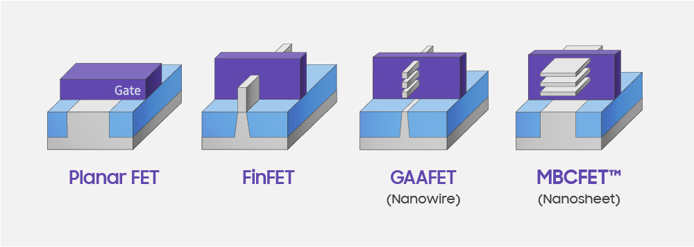
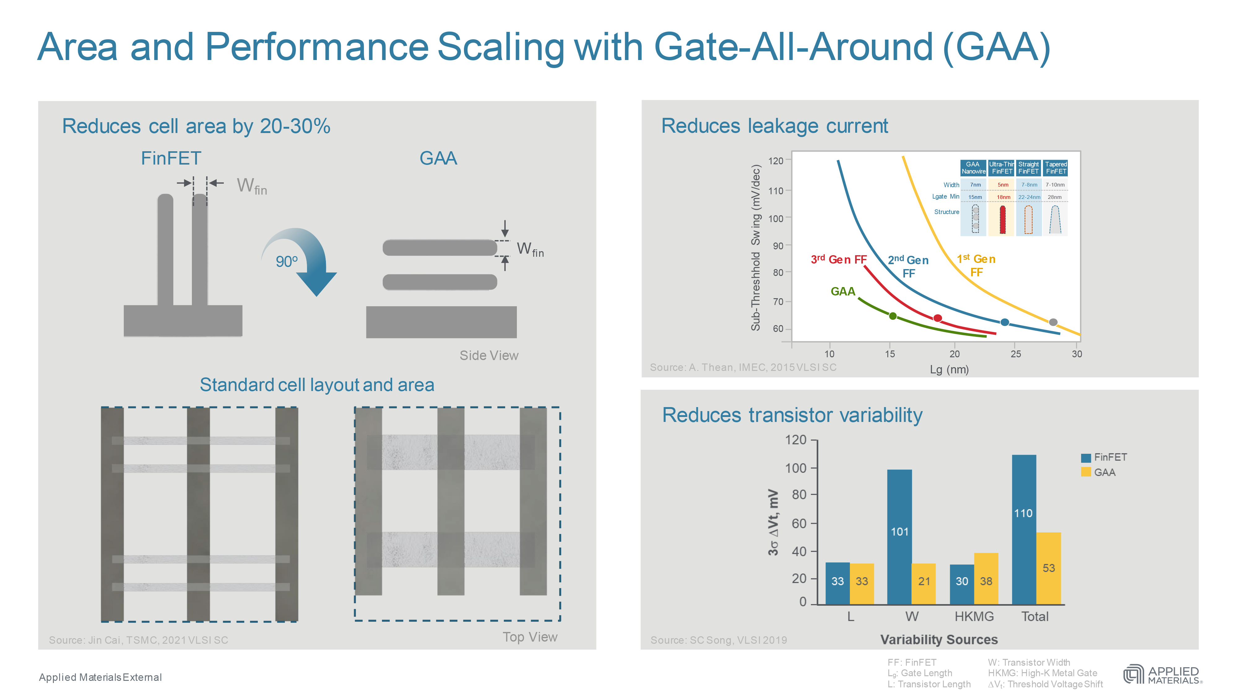
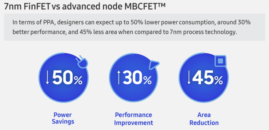
Ever since Intel introduced its 22 nm FinFET-based technology over a decade ago, chipmakers began to talk about the next inevitable step in transistor design, which is gate-all-around. As the name suggests, in GAAFETs channels are horizontal and are surrounded by gates around all four sides of the channels, which solves many problems associated with the leakage current. But this is not the only advantage: in nanosheet/nanoribbon-based GAAFETs it is possible to adjust channel width to get higher performance or reduce power consumption. Since Samsung's 3GAE and 3GAP technologies use nanosheets, Samsung calls its GAAFETs multi-bridge channel field-effect transistors (MBCFETs) to emphasize that it does not use nanowires. Furthermore, Applied Materials claims that GAA architecture reduces transistor variability, which means improved yields and faster time-to-yield (at least as far as transistor performance is concerned) and reduces cell area by 20% to 30%.
While all chipmakers have been talking about GAAFETs and their advantages over FinFETs at various academia industry events, Samsung was the first company to announce a transition to the new type of transistors with its 4 nm node sometimes in 2022 ~ 2023. Eventually, the company's plans changed a bit and in 2019 it unveiled its GAAFET-based 3GAE and 3GAP nodes with high volume manufacturing due in 2022 and 2023, respectively. Last year the company re-emphasized plans to kick off production using its 3GAE in 2022 and this quarter it said that volume production was set to start in Q2.
But Manufacturing Is Challenging
But production of chips using any leading-edge process technology is challenging and making products using Samsung's MBCFET-based 3GAE node certainly poses some risks not only because we are talking about a 3 nm-class manufacturing process, but because manufacturing of GAA transistors is different than making FinFETs.
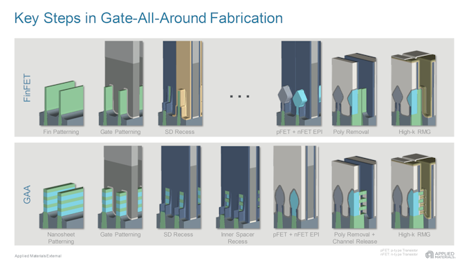
Channels of GAA transistors are shaped using lithography, epitaxy and selective materials removal, processes that enable chipmakers to fine-tune width and uniformity for optimum power and performance. Those selective materials removal and epitaxial steps are considerably more complex when compared to those with FinFETs.
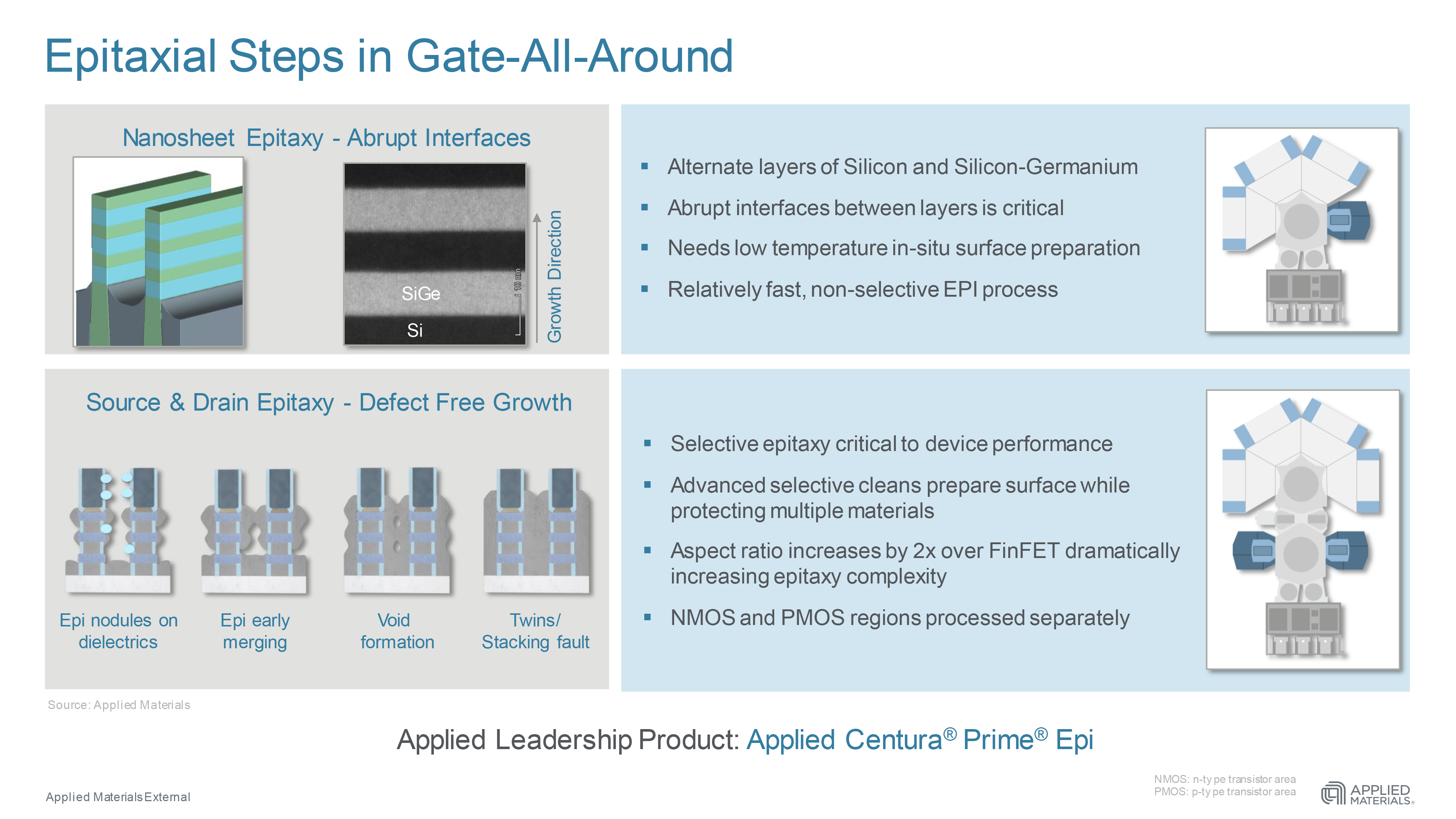
Applied's Producer Selectra Selective Etch IMS tool removes unnecessary SiGe to isolate the gate from the source/drain and define channel width without damaging surrounding materials. Applied introduced its first Selectra etching system in 2016 and since then has shipped over 1,000 chambers that are currently in use by its customers, so the industry is quite aware how to use them. While etching is a widely used process, its usage and importance will grow as the industry begins to transit to newer process technologies, including those based on GAA transistors.
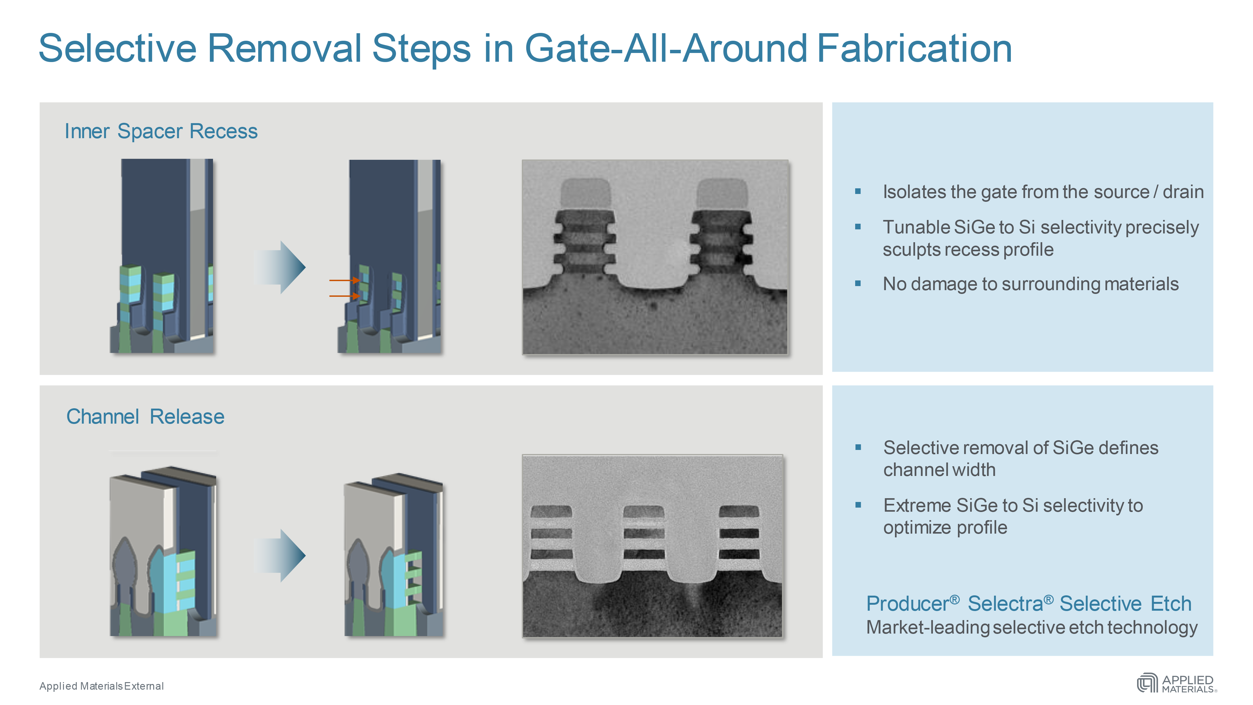
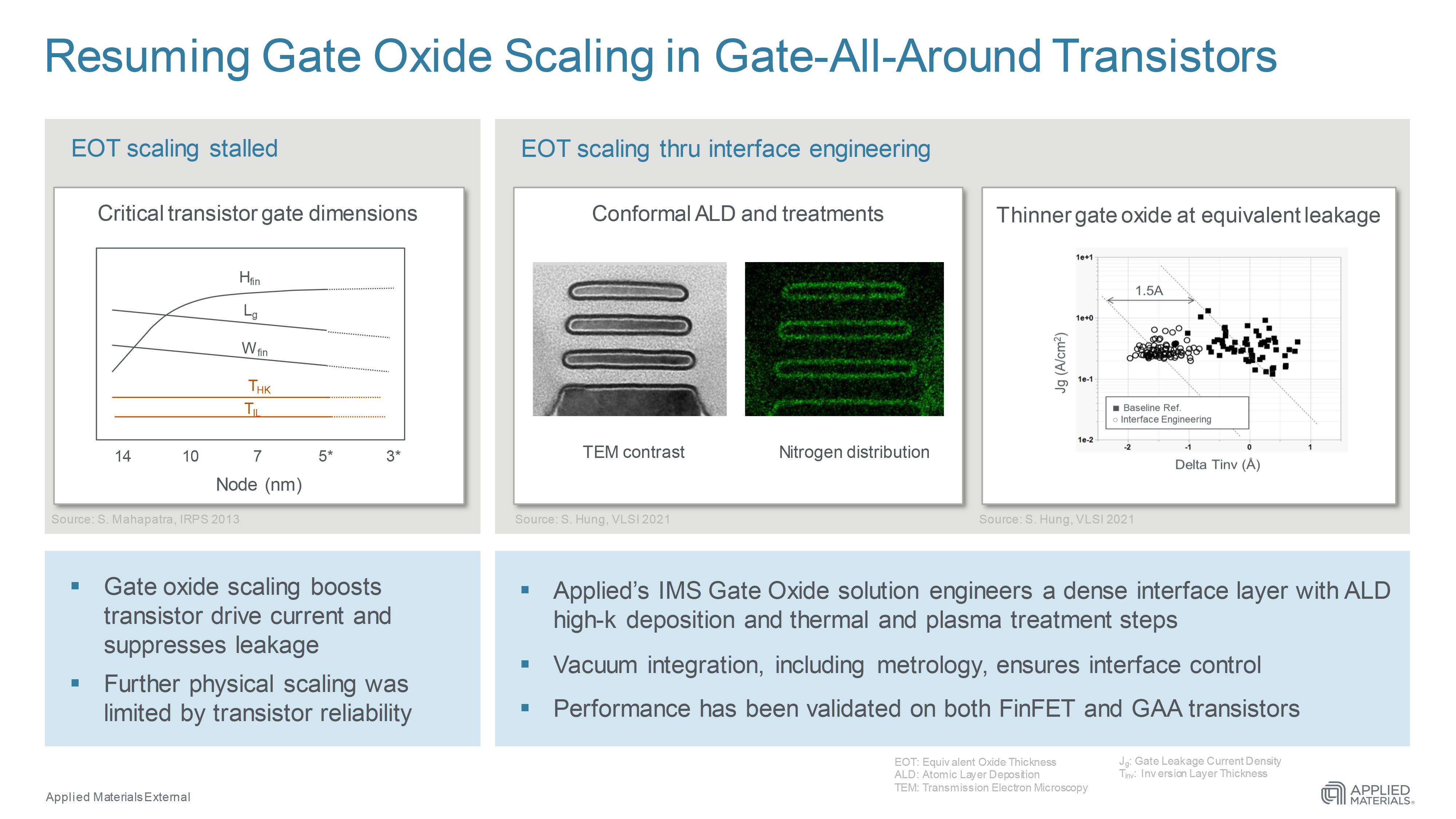
A key challenge with GAAFETs is the need to deposit the multi-layer gate oxide and metal gate stacks around the tiny 10 nm channels. This is where Applied's high-vacuum Integrated Materials Solution (IMS) systems come into play. The Applied Centura Prime Epi tool is used to deposit the Si and SiGe nanosheets with very clean and clear interfaces. Applied’s IMS system for the gate oxide stack integrates atomic layer deposition (ALD), thermal steps, plasma treatment steps, and metrology. Applied's IMS can reduce equivalent gate oxide thickness by 1.5 angstroms, enabling designers to increase performance with no increase in gate leakage or keep performance constant and reduce gate leakage by more than 10 times, the company says.
It is necessary to note that numbers shared by Applied Materials come from various companies (including TSMC, Qualcomm, IMEC, IBM, Intel, and other industry published sources) and should not be applied exclusively to Samsung Foundry's 3GAE and 3GAP nodes. Meanwhile, the general advantages of GAA/MBC/nanoribbon/nanosheet transistors, as well as challenges with their manufacturing, are similar for the whole industry.
Samsung's 3GAE: +30% Performance, -45% Area
Speaking of advantages, Samsung expects its 3GAE process to offer a 30% performance increase or a 50% power consumption reduction, and a 45% area reduction when compared to 7LPP. Such tangible benefits may be enough to justify challenges associated with this transition in the short term.
For now, the use of 3GAE manufacturing technology that relies a brand-new transistor structure is challenging in general, as in addition to new electronic design automation (EDA) tools, Samsung will need to invent new IP, and adopt brand-new design rules. All of these things, when combined with new lithography, new etching, and new deposit steps are going to make Samsung's transition difficult.
But in exchange, it will start gaining experience with GAA transistors years ahead of Intel and TSMC, which may bring certain gains in the long-term future. Furthermore, experience with GAAFETs will be beneficial for Samsung's DRAM manufacturing as memory greatly benefits from smaller cell sizes and higher transistor densities.
Source: Applied Materials


17 Comments
View All Comments
edzieba - Friday, May 13, 2022 - link
Gate oxide scaling has been stalled for a LONG time (since ~22nm). The slide notes that their solution has been validated for finFETs too, so this should bring improvements to 'traditional' processes also.TimSyd - Friday, May 13, 2022 - link
The industry has been on Hi-K dielectrics for a while now & traditional SiO2 or SiON gate materials are no longer used in nm technologies (22nm & below).Hi-K allows for physically thicker dielectric layers that have low gate leakage characteristics (tunneling etc) whilst having the equivalent electrical gate function of a much thinner gate dielectric (if had been built in traditional oxide).
So gates haven't been "oxide" for a while now. It's been a compound oxide plus Hi-K materials. With the Hi-K materials (AFAIK - Hafnium or Molybdenum compounds or other rare-earth metal combinations) getting tweaked every generation or so to slightly improve their capabilities.
FinFET gate lengths are the ones that have been slow to scale - only gradually decreasing from 28nm thru 18nm or so across 5 or 6 process generations (28, 22, 16, 12, 10, 7), with a lot of the performance gains coming from fin height instead, which effectively increases the FinFET width per unit area & hence improves drive strength.
DanNeely - Friday, May 13, 2022 - link
7nm to 3nm is several full nodes worth of nominal scaling, 45% area reduction is only 1 node worth.ballsystemlord - Friday, May 13, 2022 - link
When last I heard, Samsung was having major problems with yield[1]. Has the situation improved, or is this just an article to distract us from Samsung's problems?https://www.phonearena.com/news/samsung-execs-accu...
mode_13h - Saturday, May 14, 2022 - link
I'm always a bit apprehensive that reliability will be one of the casualties of the semiconductor process race. I tend to keep stuff for a long time, and I'd hate it if we reached a point where CPUs were simply "used up" after 5 years of average use (or maybe 1.5 years of intense use).Not only is it bad for the environment, but it could be catastrophic, in the case of a supply chain disruption even bigger than what we've experienced.
DougMcC - Saturday, May 14, 2022 - link
I think we're going to see an acceleration in the number of places where durability matters more than performance, and increasing catering to that need will follow. We'll have two tiers of computer equipment 'fast' and 'durable' and fast will be one or two orders of magnitude faster but will burn out in timescales that will require MTBF labeling, and durable will last at least decades.ballsystemlord - Sunday, May 15, 2022 - link
When you say "durable" you mean durable like the Tuf series of MBs? ;)