Intel Has Two Generations of Bitcoin ASIC: BZM1 is Built on 7nm, 137 GigaHash/sec at 2.5 W
by Dr. Ian Cutress on January 20, 2022 7:30 AM EST
It has been noted in the media that at the upcoming ISSCC conference at the end of February, Intel is set to give a talk entitled ‘Bonanza Mine: An Ultra-Low Voltage Energy Efficient Bitcoin Mining ASIC’. It already has a lot of attention, as it confirms the fact that Intel is working towards blockchain-enabling hardware. Through a number of channels, we’ve been able to acquire more details about this chip ahead of the conference.
DS1 means there's going to be a demo of it
The more compute power a miner has, the more of the blockchain rewards the miner will receive over a period of time – it always becomes a contest between the big players to get a larger share of the compute power in order to earn more rewards. Originally this went from CPUs, to GPUs, FPGAs, and now hardware designed specifically for the sole purpose of processing the blockchain and getting those awards. The current state of play regarding Bitcoin mining is led by application-specific integrated circuits, or ASICs. There are companies in the industry, such as Bitmain and MicroBT, that work with partners like TSMC to create Bitcoin-specific silicon as miners to chase the Proof-of-Work-based cryptocurrency.
AMD and NVIDIA’s hardware was used when Bitcoin mining was GPU-focused, but as the bitcoin algorithm can be accelerated further, ASICs were created. Currently those GPUs are now being used for ASIC-resistant algorithms and chains such as Ethereum, and it’s part of the reason (but not the only reason) why prices of gaming graphics cards are so high – if you can ‘earn’ enough mining to pay off the card in weeks or months, it becomes a no-brainer purchase for large mining operations. With Bitcoin however, the trend towards ASICs showcased several orders of magnitude better performance for the same power. Ultimately these proof-of-work systems get limited by how much hardware and how much power is available – Intel quoting an estimated 91TWh annual electricity use on bitcoin today (although fails to mention how that power is sourced).
ASICs inside a WhatsMiner M30S-88T, as an example
In the early days of ASICs, these were essentially FPGA-hardened IP blocks scaled up and scaled out. The need to produce and enable silicon very quickly made it very rushed to begin with, and the companies involved had limited experience of traditional silicon development and deployment timeframes. That was a number of years ago now, and some of these companies are on their 8th generation ASICs, and are leading partners at the major foundries leading-edge process technologies. The silicon is small, leading to high yields, and with the right advantage, can be very profitable. For example, Bitmain’s next-generation ASIC product installs 384 chips in a system, and in a single transaction has already sold 78000 systems (29.5m chips) to Marathon Digital Holdings for $879 million – and that’s only one customer. Sometimes in a gold rush, it’s those that sell the axes that make the money.
However in the context of the more traditional silicon players, we haven’t seen much movement on this front. The GPU vendors are fighting with miners and Ethereum, but there hasn’t really been any movement on focused silicon in this field – at least until Intel started dropping hints. Back in December, Intel’s Raja Koduri hinted that the company was moving into this space, and with the talk listed at ISSCC next month, this confirms it. But we have more details.
Intel's First Generation ASIC: BZM1
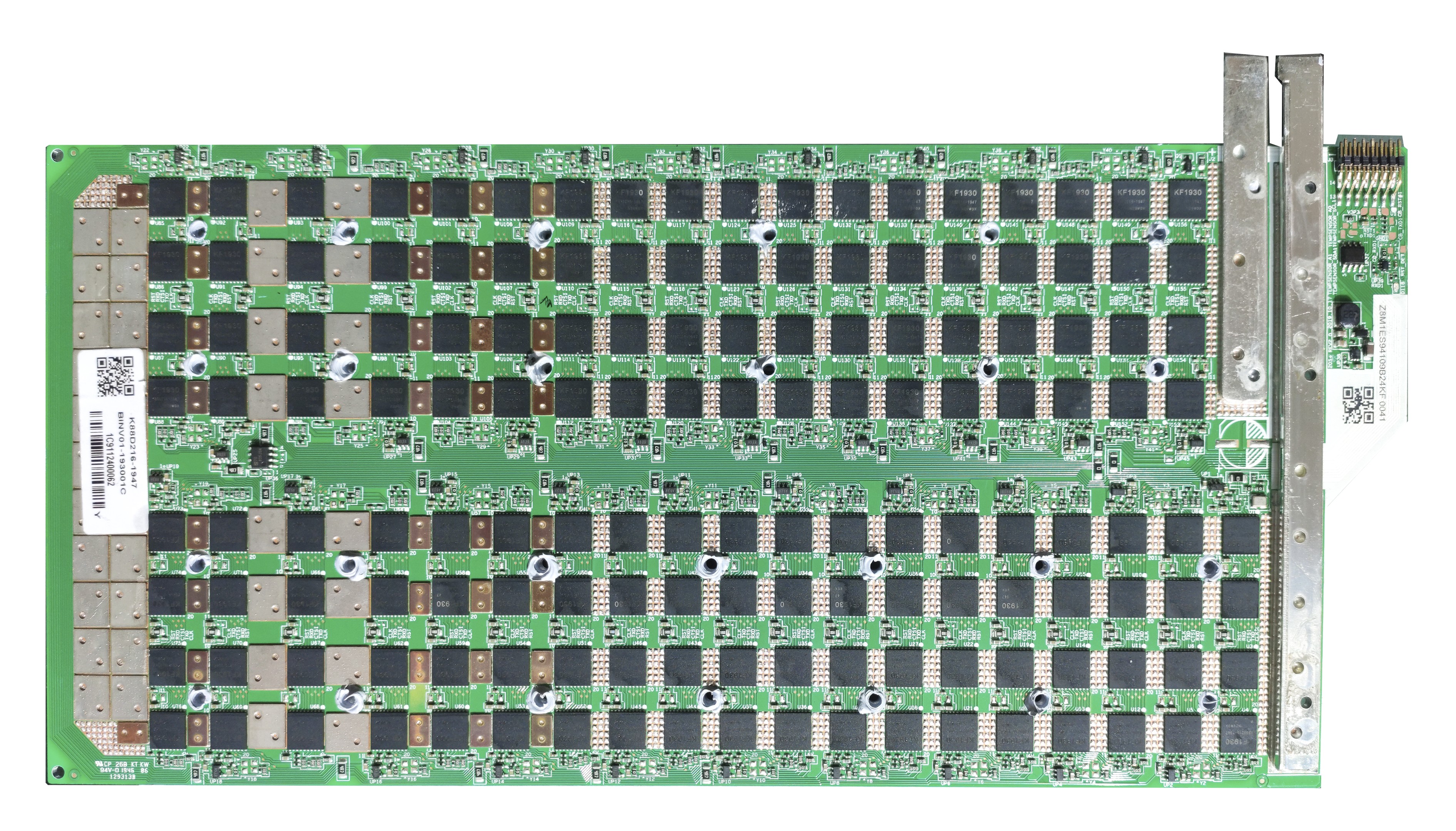
Intel has two generations of SHA-256 ASIC. The first one, BZM1, is the topic of the talk at ISSCC. Intel is building the chip on a 7nm process. Exactly which isn’t stated – the documents we have state ‘7nm’, but the same document also refers to Intel 4 as ‘4nm’. In all likelihood, this means that BZM1 is being built at Intel, and this could be one of the first IDM 2.0 customers for Intel utilizing Intel’s in-house custom design team – the SEC filing is co-signed by Intel’s GM of Custom Accelerators, for context.
The chip is 14.16 mm2 (so a maximum of 4000 chips per wafer), operates at 1.6 GHz, and generates 137 gigahash (137GH) per second at 2.5 W. 25 of these chips are used in a deep board configuration, voltage stacked at 335 mV per chip, totaling 8.875V main supply.
It’s worth noting that 335 mV per chip as a voltage minimum is insanely low. Intel says this is the most technically advanced Bitcoin ASIC to date, using an ultra-low voltage design, specialized clocking strategies, and other circuit and microarchitectural optimizations – more detail in the actual ISSCC talk in February.
Intel is going to say at ISSCC that it takes 55 J per TH, although the math here doesn't make sense given the other numbers it is presenting. At 137 GH and 2.5 W, it would mean 18.2 W/TH. For context:
| Bitcoin ASICs | ||||||
| AnandTech | Chip or System |
Hash Rate | Power | Efficiency | Node | Cost* (1 unit) |
| Intel BZM2 | Chip | ? | ? | ? | TSMC N5** | - |
| Intel BZM1 | Chip | 137 GH | 2.5 W | 18.2 W/TH | Intel 7nm | - |
| Bitmain S19j XP | Chip | ? | ? | 21.5 W/TH | TSMC N5 |
$11620 |
| System | 140 TH | 3010 W | ||||
| Bitmain S19j Pro 104T |
Chip | 270 GH | 7.99 W | 29.5 W/TH | TSMC N7 |
$11024 |
| System | 104 TH | 3068 W | ||||
| MicroBT M30S++ | Chip | 252 GH | 7.82 W | 31.0 W/TH | Samsung 8nm |
$13035 |
| System | 112 TH | 3472 W | ||||
*Cost varies with BTC. Prices listed on 1/20/2022.
**Unconfirmed Single Source of info
Intel's Second Generation ASIC: BZM2
Intel's second generation chip is listed in an SEC filing. According to the filing, it's called BZM2, and there is already a financial agreement with a customer. The filing is a four-year supply agreement between Intel and Griid Infrastructure, starting on September 8th, 2021, and the BZM2 chip is designed specifically for SHA-256 cryptographic hash functions. While exact purchase agreement numbers are redacted, Griid is to supply an 18-month rolling forecast of requested supply that Intel will work towards, with a specific reservation quantity, and a minimum deposit at the start of the agreement. These chips will be delivered up to May 2023, although the contract can be extended. Intel provides no warranty on the chips except for DOA, and also provides 3-month support after each batch of chips are delivered.
In the filing, BZM2 details are redacted.
There are two versions of BZM2, likely differing in power and performance, although the exact numbers are redacted. We have a single source that states BZM2 is being built on TSMC N5, offering 35 J/TH, which by the same metric would be a 37% power saving over the first generation. This information may not be correct however; we are looking to second source it.
We're unsure why Intel is giving a talk about its first generation chip at ISSCC when it is already taking orders for its second generation hardware - it might simply be because Intel does not want to disclose detail about its leading edge hardware. This is despite Intel's new CEO Pat Gelsinger often repeating the pledge to be more open.
The Competition and Market
Bitmain’s latest generation is built on TSMC N5, showcases almost the same efficiency. We ran the numbers back from the S19j Pro 104, built on TSMC N7, knowing that a full system contains 384 chips at 2750-3250 W. It equates to around 7-8 W per chip, which is 3x what Intel is suggesting their chip can do. We're also seeing reports that these TSMC N7 chips are over a billion transistors each. In order to compete for density then, we’re going to see systems with 2-3x more chips. It’s going to be a way for Intel to fill up its 7nm fabs with small high-yielding silicon at any rate.
It’s worth noting that if Intel had an order for 29.5 million chips (as noted above, for $867m), at perfect yield at 4000 per wafer, it would take almost 7500 wafers. Intel quotes market research that says that it expects the cryptocurrency mining hardware market to grow by $2.8B during 2021-2025.
I spoke with a colleague who focuses more on the mining/ASIC space, and he stated that it’s likely having US-based ASIC production is a benefit for locality, language and relations, and avoiding additional 25% tariffs currently on mining hardware. My guess is that Intel will be working with specific partners that have minimum order requirements for this sort of hardware.
It’s unlikely to mean much for the beleaguered GPU market – just hope they don’t put one on the GPU board as a way to help miners ‘recoup’ the cost of the GPU itself. We're in a good timeline, right?
If anyone has die sizes of competing ASICs in the market, please let me know.
Update: Last week, one of Intel's Senior Directors, we believe the director of Custom Accelerators, was hired by Bitfury.
Update 2: Intel reached out to inform us that the ISSCC talk is regarding their first generation BZM1 ASIC. The agreement with Griid is for its second generation BZM2 ASIC, which will be discussed at a later date. The article has been updated to clarify this.


107 Comments
View All Comments
onewingedangel - Thursday, January 20, 2022 - link
Great way for Intel to sell test wafers on a developing process.shabby - Thursday, January 20, 2022 - link
Isn't that what the mobile chips are for?James5mith - Thursday, January 20, 2022 - link
"Sometimes in a gold rush, it’s those that sell the axes* that make the money."*Pickaxes, not axes.
Ian Cutress - Thursday, January 20, 2022 - link
In this case, I absolutely mean axes.waterdog - Thursday, January 20, 2022 - link
I understood and appreciated it. :)FullmetalTitan - Thursday, January 20, 2022 - link
So instead of fixing the managerial rot, Intel has decided to announce they are enabling even MORE shitcoin mining?Seems like exactly their kind of head-in-ass decision making
Unashamed_unoriginal_username_x86 - Thursday, January 20, 2022 - link
Pop the bubble! Pop the bubble!Unashamed_unoriginal_username_x86 - Thursday, January 20, 2022 - link
I'm not sure if the spam filter's changed but I like this explanationhttps://www.twitch.tv/videos/1259714412?t=00h57m24...
TomWomack - Thursday, January 20, 2022 - link
Doing anything with a 335mV supply is quite impressive; and there's a lot of cojones in an implementation piling up Intel 7 custom silicon 25 deep so as to be able to use a single nine-volt 7.5-amp regulator per PCB rather than carefully distributing 7.5A @ 335mV to each chip!TomWomack - Thursday, January 20, 2022 - link
I mean, I thought it was quite a fine cheap trick to pile up 3.5V LEDs 30-deep and connect unrectified 110V mains to pairs of strings in opposite directions, so the LEDs were their own voltage dividers, and the strings shone on alternate phases. This is doing the same with things much more expensive than LEDs!