How Low Cost Can Chiplets Go? Depends on the Optimization, says AMD’s CEO Dr. Lisa Su
by Dr. Ian Cutress on January 14, 2022 10:00 AM EST- Posted in
- CPUs
- AMD
- APUs
- Trade Shows
- SoCs
- Lisa Su
- Interviews
- CES 2022
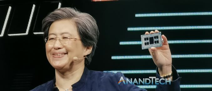
While not the absolute first company in the market to talk about putting different types of silicon inside the same package, AMD’s launch of Ryzen 3000 back in July 2019 was a first in bringing high performance x86 computing through the medium of chiplets. The chiplet paradigm has worked out very well for the company, having high performance cores on optimized TSMC 7nm silicon, while farming the more analog operations to cheaper GlobalFoundries 14nm silicon, and building a high speed interconnect between them. Compared to a monolithic design, AMD ends up using the better process for each feature, smaller chips that afford better yields and binning, and the major cost adder becomes the packaging. But how low cost can these chiplet designs go? I put this question to AMD’s CEO Dr. Lisa Su.
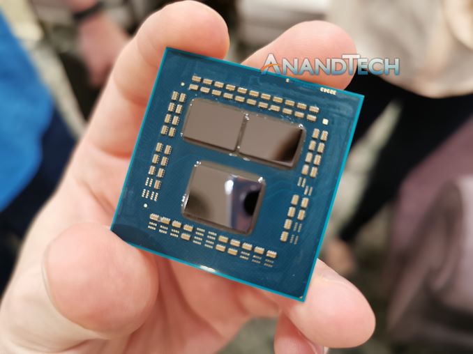
In AMD’s consumer-focused product stack, the only products it ships with chiplets are the high-performance Ryzen 3000 and Ryzen 5000 series processors. These range in price from $199 for the six-core Ryzen 5 3600, up to $799 for the 16-core Ryzen 9 5950X.
Everything else consumer focused is a single piece of silicon, not chiplets. Everything in AMD’s mobile portfolio relies on single pieces of silicon, and they are also migrated into desktop form factors in AMD’s desktop APU strategy. We’re seeing a clear delineation between where chiplets make financial sense, and where they do not. From AMD’s latest generation of processors, the Ryzen 5 5600X is still a $299 cost at retailers.
One of the issues here is that a chiplet design requires additional packaging steps. The silicon from which these processors are made have to sit in a PCB or substrate, and depending on what you want to do with the substrate can influence its cost. Chiplet designs require high speed connections between chiplets, as well as power and communications to the rest of the system. The act of putting the chiplets on a singular substrate also has an effective cost, requiring accuracy - even if 99% accurate placement per chiplet on a substrate means a 3 chiplet product as a 3% yield loss from packaging, raising costs. Beyond this, AMD has to ship its 14nm dies for its products from New York to Asia first, to package them with the TSMC compute dies, before shipping the final product around the world. That might be reduced in future, as AMD is believed to make its next-generation chiplet designs all within Asia.
Ultimately there has to be a tipping point where simply building a monolithic silicon product becomes better for total cost than trying to ship chiplets around and spend lots of money on new packaging techniques. I asked the question to Dr. Lisa Su, acknowledging that AMD doesn’t sell its latest generation below $300, as to whether $300 is the realistic tipping point from the chiplet to the non-chiplet market.
Dr. Su explained how in their product design stages, AMD’s architects look at every possible way of putting chips together. She explained that this means monolithic, chiplet, packaging, process technologies, as the number of potential variables in all of this have direct knock-on effects for supply chain and cost and availability, as well as the end performance of the product. Dr. Su stated quote succinctly that AMD looks for what is best for performance, power, cost – and what you say on the tipping point may be true. That being said, Dr. Su was keen not to directly say this is the norm, detailing that she would expect in the future that the dynamic might change as silicon costs rise, as this changes that optimization point. But it was clear in our discussions that AMD is always looking at the variables, with Dr. Su ending on a happy note that at the right time, you’ll see chiplets at the lower end of the market.
Personally, I think it’s quite telling that the market is very malleable to chiplets right now in the $300+ ecosystem. TSMC D0 yields of N7 (and N5) are reportedly some of the industry best, which means that AMD’s mobile processors in the ~200 sq mm range can roll off the production line and cater for everything up to that $300 value (and perhaps some beyond). Going bigger brings in die size yield constraints, where chiplets make sense. We’re now in at a stage where if Moore’s Law continues, how much compute can we fit in that 200 sq mm sized silicon, and which markets can benefit from it – or are we going to get to a point where so many more features are added that silicon sizes would increase, necessarily pushing everything down the chiplet route. As part of the discussion, Dr. Su mentioned economies of scale when it comes to packaging, so it will be interesting to see how this dynamic shakes out. But for now it seems, AMD’s way to address the sub-$300 market is going to be with either last generation hardware, or monolithic silicon.
This article was updated to clear up some of the language around certainty and conjecture based on rumor.


55 Comments
View All Comments
mode_13h - Sunday, January 16, 2022 - link
AMD has more constraints on production capacity than Intel. I'm sure they'd like to address all market segments, but they have to be judicious about where to allocate their dies.TekCheck - Sunday, January 16, 2022 - link
They are not interested in covering every segment of the market. It is not necessary. Besides, there is just as much as you could possibly cover. Do not forget that AMD had been posting historically record revenues. They are literally selling everything they could possibly produce.Once their capacity increases, they will be able to cover more segments.
Alexvrb - Saturday, January 15, 2022 - link
"Beyond this, AMD has to ship its 14nm dies for its products from New York to Asia first, to package them with the TSMC compute dies, before shipping the final product around the world. That might be reduced in future, as AMD is believed to make its next-generation chiplet designs all within Asia."Hmm, on the surface that seems unlikely, given the recent extension of their deal with GF. What would they do with all the excess wafer supply? I doubt shipping adds much cost on a per-chip basis to start with.
casteve - Monday, January 17, 2022 - link
Yeah, the shipping comment is a bit inane. The silicon is all air shipped - not on some banana boat. So, a few days to get there and clear customs. It's going to be shipped as die in wafer form and then assembled with all the rest. Depending on the arrangement with the foundry, it might be tested die shipped or raw wafers shipped and tested in Asia.TekCheck - Sunday, January 16, 2022 - link
My question is regarding Rembrandt. The platform is marketed as DisplaytPort 2.0 "Ready". What does this really mean? I can neither see that RDNA2 iGPU supports UHBR10 output at 40 Gbps not dGPU supporitng anything more than DP 1.4. Is there any level shifter chip on motherboard that supports DP 2.0 at 40 Gbps? "Ready" always worries me that something is not there quite yet.