The Snapdragon 8 Gen 1 Performance Preview: Sizing Up Cortex-X2
by Dr. Ian Cutress on December 14, 2021 8:00 AM EST
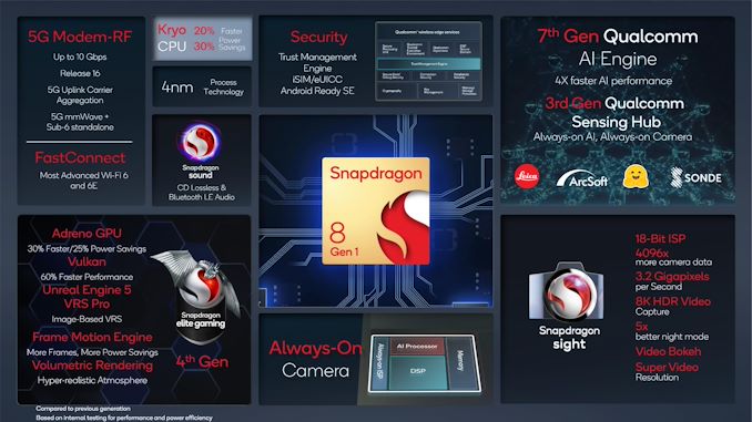
At the recent Qualcomm Snapdragon Tech Summit, the company announced its new flagship smartphone processor, the Snapdragon 8 Gen 1. Replacing the Snapdragon 888, this new chip is set to be in a number of high performance flagship smartphones in 2022. The new chip is Qualcomm’s first to use Arm v9 CPU cores as well as Samsung’s 4nm process node technology. In advance of devices coming in Q1, we attended a benchmarking session using Qualcomm’s reference design, and had a couple of hours to run tests focused on the new performance core, based on Arm’s Cortex-X2 core IP.
The Snapdragon 8 Gen 1
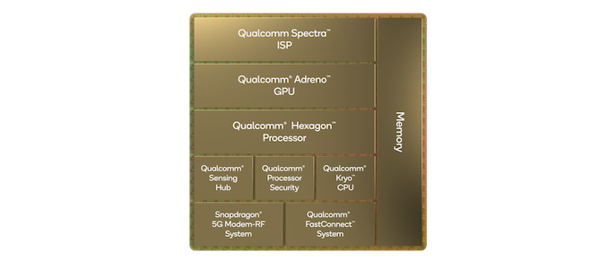
Rather than continue with the 800 naming scheme, Qualcomm is renaming its smartphone processor portfolio to make it easier to understand / market to consumers. The Snapdragon 8 Gen 1 (hereafter referred to as S8g1 or 8g1) will be the headliner for the portfolio, and we expect Qualcomm to announce other processors in the family as we move into 2022. The S8g1 uses the latest range of Arm core IP, along with updated Adreno, Hexagon, and connectivity IP including an integrated X65 modem capable of both mmWave and Sub 6 GHz for a worldwide solution in a single chip.
While Qualcomm hasn’t given any additional insight into the Adreno / graphics part of the hardware, not even giving us a 3-digit identifier, we have been told that it is a new ground up design. Qualcomm has also told us that the new GPU family is designed to look very similar to previous Adreno GPU sfrom a feature/API standpoint, which means that for existing games and other apps, it should allow a smooth transition with better performance. We had time to run a few traditional gaming tests in this piece.
On the DSP side, Qualcomm’s headlines are that the chip can process 3.2 Gigapixels/sec for the cameras with an 18-bit pipeline, suitable for a single 200MP camera, 64MP burst capture, or 8K HDR video. The encode/decode engines allow for 8K30 or 4K120 10-bit H.265 encode, as well as 720p960 infinite recording. There is no AV1 decode engine in this chip, with Qualcomm’s VPs stating that the timing for their IP block did not synchronize with this chip.
AI inference performance has also quadrupled - 2x from architecture updates and 2x from software. We have a couple of AI tests in this piece.
As usual with these benchmarking sessions, we’re very interested in what the CPU part of the chip can do. The new S8g1 from Qualcomm features a 1+3+4 configuration, similar to the Snapdragon S888, but using Arm’s newest v9 architecture cores.
- The single big core is a Cortex-X2, running at 3.0 GHz with 1 MiB of private L2 cache.
- The middle cores are Cortex-A710, running at 2.5 GHz with 512 KiB of private L2 cache.
- The four efficiency cores are Cortex-A510, running at 1.8 GHz and an unknown amount of L2 cache. These four cores are arranged in pairs, with L2 cache being private to a pair.
- On the top of these cores is an additional 6 MiB of shared L3 cache and 4 MiB of system level cache at the memory controller, which is a 64-bit LPDDR5-3200 interface for 51.2 GB/s theoretical peak bandwidth.
Compared to the Snapdragon S888, the X2 is clocked higher than the X1 by around 5% and has additional architectural improvements on top of that. Qualcomm is claiming +20% performance or +30% power efficiency for the new X2 core over X1, and on that last point it is beyond the +16% power efficiency quoted by Samsung moving from 5nm to 4nm, so there are additional efficiencies Qualcomm is implementing in silicon to get that number. Unfortunately Qualcomm would not go into detail what those are, nor provide details about how the voltage rails are separated, if this is the same as S888 or different – Arm has stated that the X2 core could offer reduced power than the X1, and if the X2 is on its own voltage rail that could provide support for Qualcomm’s claims.
The middle A710 cores are also Arm v9, with an 80 MHz bump over the previous generation likely provided by process node improvements. The smaller A510 efficiency cores are built as two complexes each of two cores, with a shared L2 cache in each complex. This layout is meant to provide better area efficiency, although Qualcomm did not explain how much L2 cache is in each complex – normally they do, but for whatever reason in this generation it wasn’t detailed. We didn’t probe the number in our testing here due to limited time, but no doubt when devices come to market we’ll find out.
On top of the cores is a 6 MiB L3 cache as part of the DSU, and a 4 MiB system cache with the memory controllers. Like last year, the cores do not have direct access to this 4 MiB cache. We’ve seen Qualcomm’s main high-end competitor for next year, MediaTek, showcase that L3+system cache will be 14 MiB, with cores having access to all, so it will be interesting to see how the two compare when we have the MTK chip to test.
Benchmarking Session: How It Works
For our benchmarking session, we were given a ‘Qualcomm Reference Device’ (QRD) – this is what Qualcomm builds to show a representation of how a flagship featuring the processor might look. It looks very similar to modern smartphones, with the goal to mirror something that might come to market in both software and hardware. The software part is important, as the partner devices are likely a couple of months from launch, and so we recognize that not everything is final here. These devices also tend to be thermally similar to a future retail example, and it’s pretty obvious if there was something odd in the thermals as we test.
These benchmark sessions usually involve 20-40 press, each with a device, for 2-4 hours as needed. Qualcomm preloads the device with a number of common benchmarking applications, as well as a data sheet of the results they should expect. Any member of the press that wants to sideload any new applications has to at least ask one of the reps or engineers in the room. In our traditional workflow, we sideload power monitoring tools and SPEC2017, along with our other microarchitecture tests. Qualcomm never has any issue with us using these.
As with previous QRD testing, there are two performance presets on the device – a baseline preset expected to showcase normal operation, and a high performance preset that opportunistically puts threads onto the X2 core even when power and thermals is quite high, giving the best score regardless. The debate in smartphone benchmarking of initial runs vs. sustained performance is a long one that we won’t go into here (most noticeably because 4 hours is too short to do any extensive sustained testing) however the performance mode is meant to enable a ‘first run’ score every time.


169 Comments
View All Comments
rtho782 - Friday, December 17, 2021 - link
Alex Katouzian is like budget Sylvester Stallone :Dbogamia - Monday, December 20, 2021 - link
Apparently, D9000 has been benchmarked by this Chinese YouTuber (https://youtu.be/1ves1M4Ai-I) and it outperformed the snapdragon 8 gen 1 in all the areas. The performance power watt gap is massive between these two chips. Even in GPU benchmarks, D9000 outperformed the snapdragon equivalent. This is going to be an interesting generation. I wonder what will be the excuses of OEMs to use Qualcomm in the affordable flagship segments .iphonebestgamephone - Monday, December 20, 2021 - link
It looks like things like genshin impact is still more optimized for adreno.ChrisGX - Thursday, December 23, 2021 - link
>>[the D9000] outperformed the snapdragon 8 gen 1 in all the areas<<Not, exactly. The vlogger makes clear that the Adreno GPU in the Snapdragon 8 Gen 1 offers slightly higher performance than the Mali G710 in the D9000 but that the small performance increment comes at a significant cost in power consumption terms. So, while the Mali GPU offers slightly lower performance it is definitely the more energy efficient GPU.
Kangal - Friday, December 24, 2021 - link
Interesting video. Here's the recap:GeekBench 5 (Single-core)
D9000: 1287 score, 3.5 Watts, 368 Efficiency
QC 8g1: 1200 score, 4.2 Watts, 286 Efficiency
QSD 888: 1135 score, 3.8 Watts, 299 Efficiency
GeekBench 5 (Multi-thread)
D9000: 4474 score, 9.8 Watts, 457 Efficiency
QC 8g1: 3810 score, 11.1 Watts, 343 Efficiency
QSD 888: 3753 score, 8.9 Watts, 422 Efficiency
GFXBench Aztec Ruins (High/1440p Offscreen)
D9000: 43 fps, 8.2 Watts, 5.24 Efficiency
QC 8g1: 47 fps, 11.2 Watts, 4.20 Efficiency
QSD 888: 30 fps, 9.0 Watts, 3.34 Efficiency
Genshin Impact (Quality Mode, Initial Performance)
D9000: 60 fps, 6.8 Watts, drops 1.1 Watts, 7 minutes then throttles
QC 8g1: 60 fps, 7.5 Watts, drops 1.2 Watts, 3 min then dips but maintains
QSD 888: 60 fps, 7.5 Watts, drops 1.6 Watts, 6 minutes then throttles
Genshin Impact (Quality Mode, after 15min throttling)
D9000: 48 fps, 5.7 Watts, 8.42 Efficiency, Resolution 1422x640
QC 8g1: 55 fps, 6.3 Watts, 8.73 Efficiency, Resolution 1422x640
QSD 888: 48 fps, 5.9 Watts, 8.14 Efficiency, Resolution 1600x720
ChrisGX - Tuesday, January 4, 2022 - link
Xiaobai's Tech Reviews ( https://www.youtube.com/watch?v=_TyEkQZvAEI ) - a Hong Kong based YouTuber - has come to similar conclusions to the tech vlogger (Geekerwan) that you cite. The benchmark testing conducted by both vloggers seems broader in scope and more careful than the usual fare on YouTube. In both cases the engineering test mules/prototype devices tested were equipped with the latest crop of premium ARM SoCs (that will appear in production Android devices in 2022). The similarity of benchmark results doesn't guarantee the correctness of those results or the completeness of the performance picture drawn, of course, but with independent sources getting very similar results it wouldn't be a shock if production devices follow the evident pattern.Golden Reviewer, a Singapore based tech reviewer/vlogger (posting reviews in English) if anything offers an even more critical account of the SD8 Gen 1 and an account of the D9000 that does indeed credit it as the better chip in most areas. Using a pre-production device in testing he singles out overheating as a serious problem for the SD8 Gen 1.
https://www.youtube.com/watch?v=HO46vmsS61Y
https://www.youtube.com/watch?v=dCYx3K4qjX4
https://www.youtube.com/watch?v=bTW6Z55bEfU
maik80 - Tuesday, January 18, 2022 - link
Fans of android have a mania to use AnTuTu, the owner has already been arrested for fraud in the tests, it has already been confirmed that he received to increase the result. In addition to giving points for the amount of ram memory. it's a jokeqnfw3174 - Thursday, March 31, 2022 - link
Is it finished to test A710/A510? Where can I find the result?yeeeeman - Monday, April 25, 2022 - link
Can we get a follow up on this?