Supermicro Ultra SYS-120U-TNR Review: Testing Dual 10nm Ice Lake Xeon in 1U
by Dr. Ian Cutress on July 22, 2021 9:00 AM ESTBIOS, Software, BMC
The networked management for the Supermicro SYS-120U-TNR uses the latest interface from Supermicro through the ASpeed AST2600 which is given an IP my DHCP upon connection. Interestingly enough trying to access the interface did not work with Chrome at all - after logging in it would just freeze on the system page while trying to get basic system details. In the end I had to use non-Chromium based Edge. On top of that both Chrome and Edge warned that the certificate for the BMC webpage was invalid, resulting in jumping through a hoop to access it.
The username and password to access the system are no longer the default admin/admin or admin/password: due to the 2018 law in California known as SB-327, all IoT devices (including servers) that have administrator access to settings and configurations must have unique passwords. The username for us was still ADMIN however the password was found on a pull-out tab on the front of the server - or alternatively just on the inside of the double width PCIe slot inside the chassis.
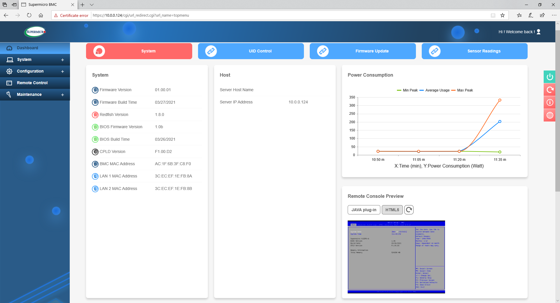
The Supermicro interface is as detailed as a management interface needs to be, with this main dashboard showcasing firmware versions, power consumption, the remote console, and recent system messages and actions.
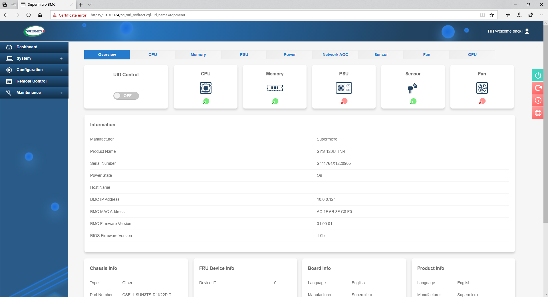
The System tab states a lot of similar information to the dashboard, with links to the separate component detection of the server.
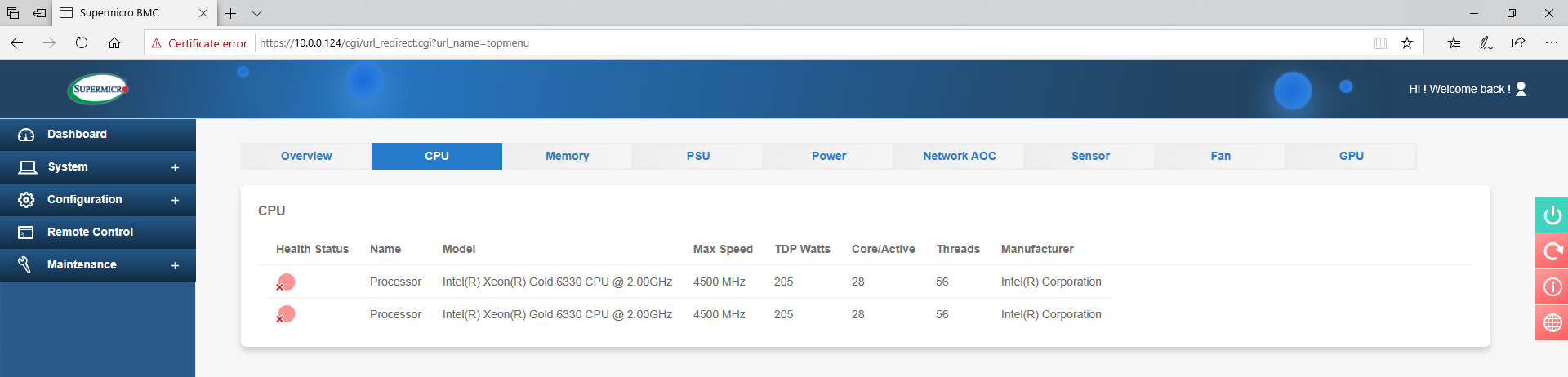
The CPUs are both detected here, and although it says they have with a base frequency of 2.00 GHz (actually 2.6 GHz) and a turbo frequency of 4.5 GHz (actually 3.1 GHz), we actually measure the correct numbers in the operating system.

All sixteen memory modules are detected, with ECC enabled, for a total of 512 GB.
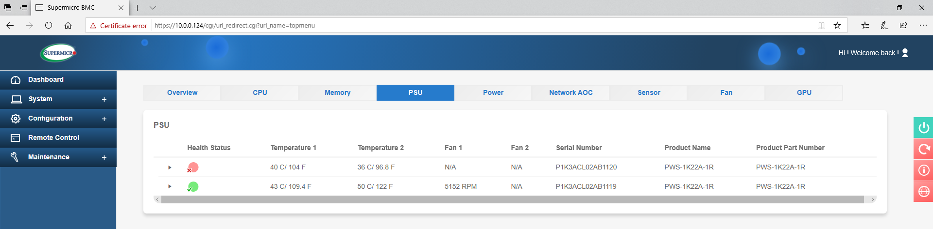
Power supplies as well – in this image we only have one of the 1200W models connected to the mains, but even without it will still showcase the thermal sensor on the power supply not connected.
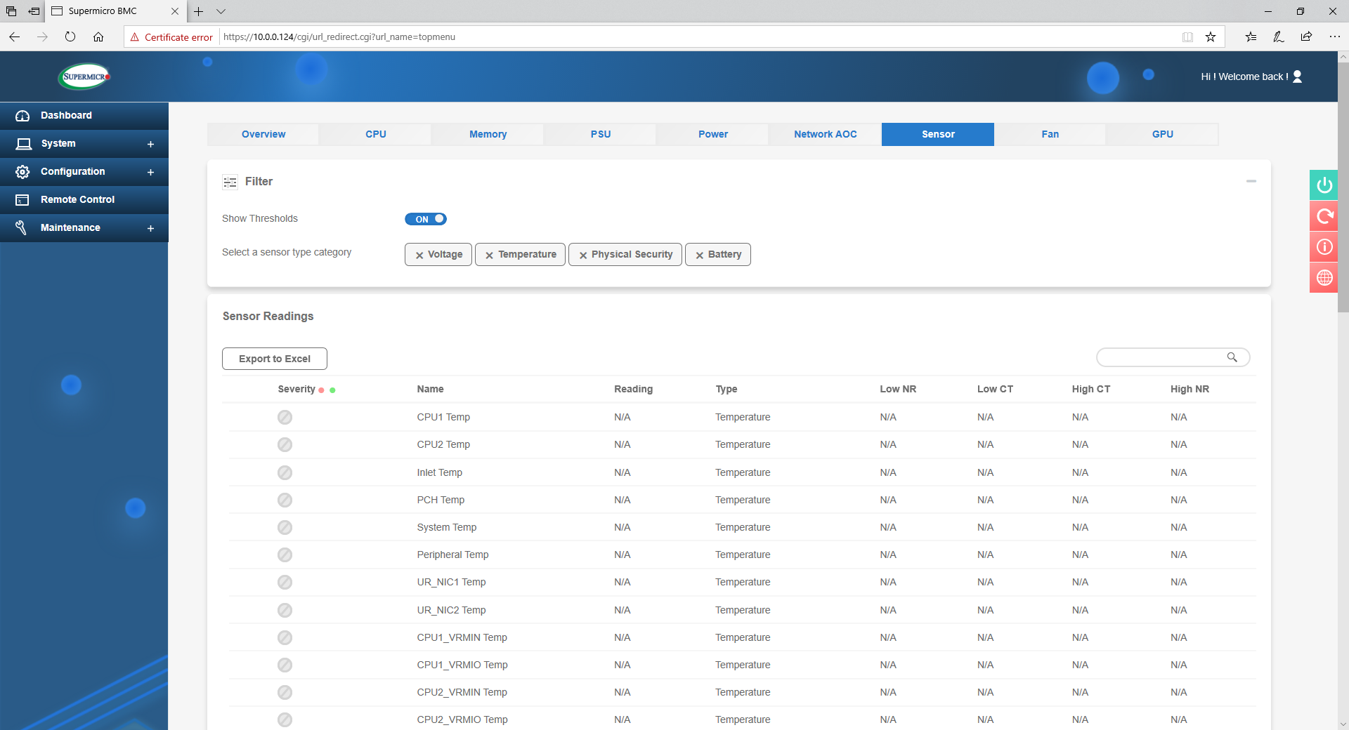
In our system, the sensor module didn’t seem to read anything from the hardware, however we did run the fans at full speed regardless.
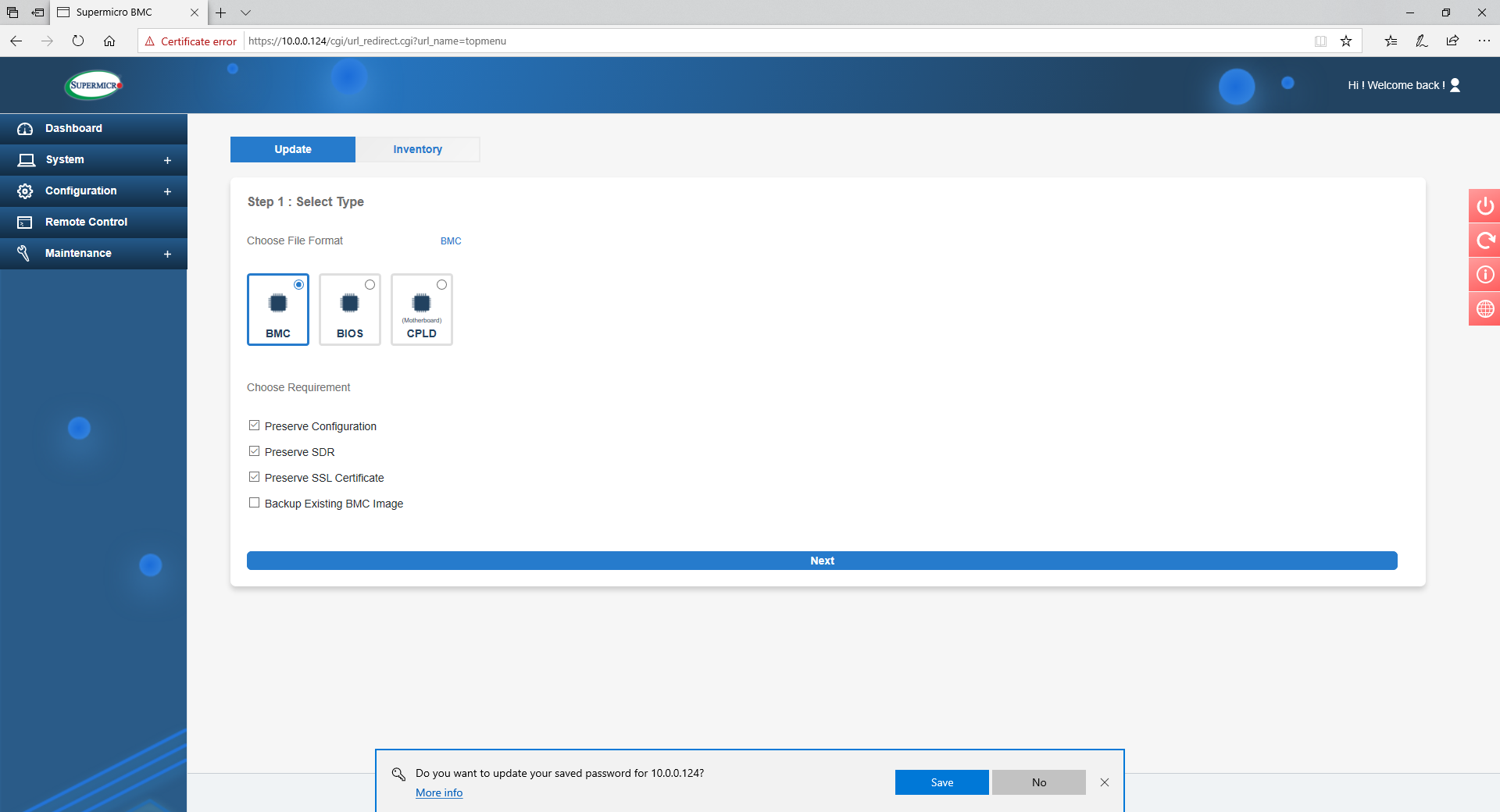
Updating the BMC or BIOS is relatively easy through the update interface when you have a file to hand. The system also keeps track of when it was updated and with what version firmware.

For remote control, both HTML5 and Java are supported, however we could not get the HTML 5 interface to work during our testing. Java worked well, and is likely kept here for the specific reason of legacy and fallback support despite Java not being recommended.
Overall the management options were as standard as we normally expect from this sort of system. On the plus side it looks a lot nicer than some of the base AMI / older interfaces we still encounter from time to time, but on the minus side I’m still unsure why it wouldn’t work in Chrome.
 Power_thumb.png)
 Main_thumb.png)
 System_thumb.png)
 CPU_thumb.png)
 Memory_thumb.png)
 PSU_thumb.png)
BIOS
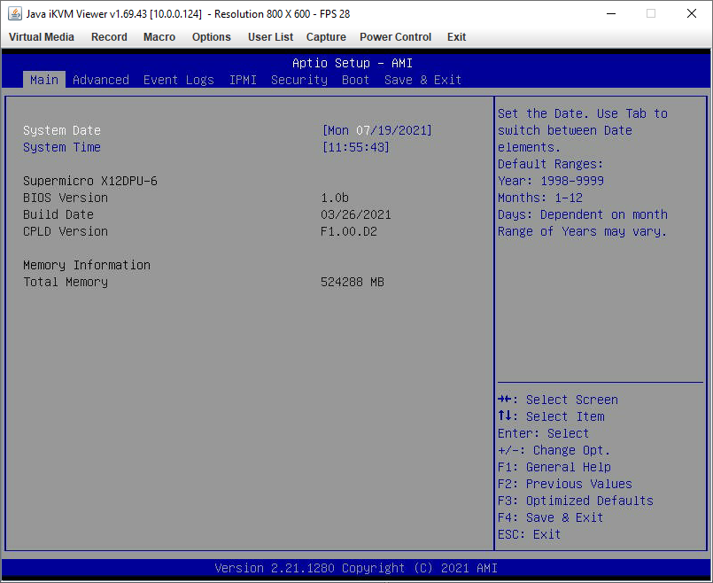
On the BIOS/UEFI side of the equation, we get a simple blue and grey interface from AMI which runs as standard on enterprise systems. The X12DPU-6 motherboard we are using has BIOS version 1.0b and a total of 512 GB of memory detected.
In the Advanced CPU section, it showcases that we have two Xeon Gold 6330 processors, with the D1 stepping. Similar to the BMC, it says here a 2.0 GHz base frequency (Intel’s official specifications state 2.5 GHz) but everything else looks in order. Individual cores can be disabled with the bitmaps as shown here:
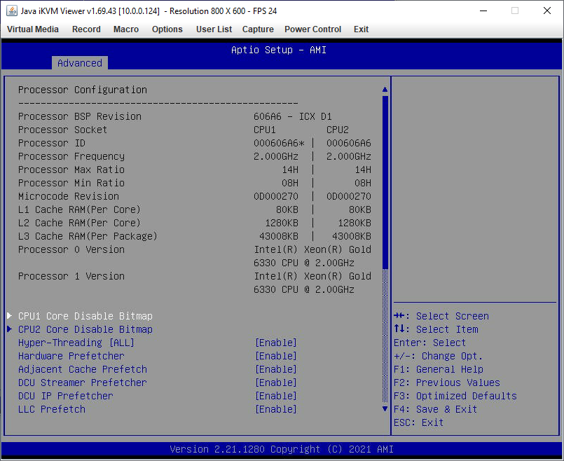
One of the new features of the Xeon Gold processors is SGX enclaves, which require TME to be enabled.
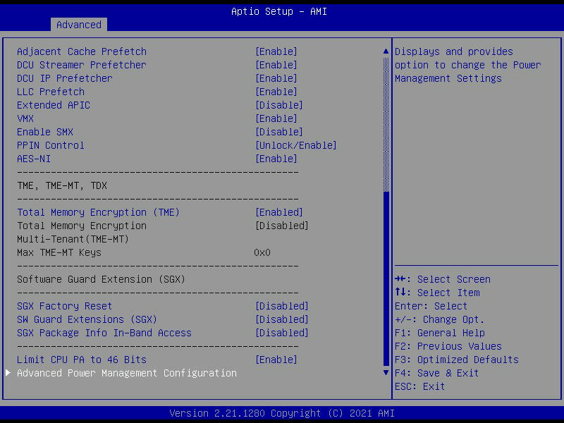
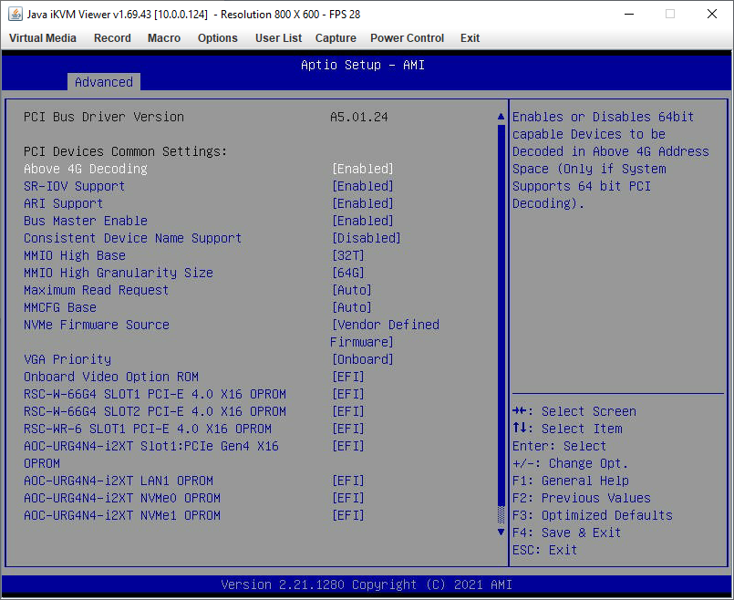
In the PCIe section, Above 4G Decoding was enabled by default (often disabled by default on consumer platforms), and the system allows a selection of NVMe firmware such that it can be software driven rather than vendor firmware driven.
For the uncore / mesh sub-system, we can see that this system is configured to 11.2 GT/s speed UPI links (one of the upgrades over previous generation), but there are also a number of options here that could affect the system based on use case. Customers can select the system to prioritize topologically at the expense of feature performance (e.g. cores over IO), or vice versa. Similarly a user can select SNC2 (Sub-NUMA Clustering) to partition the processor into two hemispheres for lower latency memory accesses at the expense of immediate bandwidth. There is also an option to throttle cache snooping to manage power based on what sort of workloads the system would end up running.

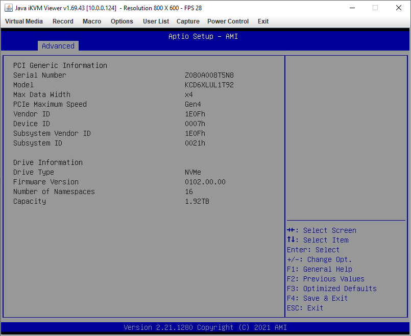
All the NVMe slots in the front panel of the system can be PCIe 4.0 x4 enabled, and there’s an option to check that here as well.
Other options in the BIOS include IMPI network settings, event logs, and traditional BIOS security.
 - Main_thumb.png)
 - Advanced_thumb.png)
 - Boot Feature_thumb.png)
 - CPU1_thumb.png)
 - CPU2_thumb.png)
 - PCIe_thumb.png)


53 Comments
View All Comments
Elstar - Saturday, July 24, 2021 - link
> All I want to do is see if people can close the gap between AVX2 and AVX-512 somewhat, or at least explain why it's as big as it is. Maybe there's some magic AVX-512 instructions that have no equivalent in AVX2, which turn out to be huge wins. It would at least be nice to know.AVX-512, as an instruction set, was a huge leap forward compared to AVX/AVX2. So much so that Intel created the AVX-512VL extension that allows one to use AVX-512 instructions on vectors smaller than 512-bits. As a vector programmer, here are the things I like about AVX-512:
1) Dedicated mask registers and every instruction can take an optional mask for zeroing/merging results
2) AVX-512 instructions can broadcast from memory without requiring a separate instruction.
3) More register (not just wider)
Also, and this is kind of hard to explain, but AVX/AVX2 as an instruction set is really annoying beacause it acts like two SSE units. So for example, you can't permute (or "shuffle" in Intel parlance) the contents of an AVX2 register as a whole. You can only permute the two 128-bit halves as if they were/are two SSE registers fused together. AVX-512 doesn't repeat this half-assed design approach.
mode_13h - Sunday, July 25, 2021 - link
> 1) Dedicated mask registers and every instruction can take an optional> mask for zeroing/merging results
This seems like the only major win. The rest are just chipping at the margins.
More registers is a win for cases like fitting a larger convolution kernel or matrix row/column in registers, but I think it's really the GP registers that are under the most pressure.
AVX-512 is not without its downsides, which have been well-documented.
Spunjji - Monday, July 26, 2021 - link
@Elstar - Interesting info. Just makes me more curious as to how many of these things might be benefiting the 3DPM workload specifically. Another good reason for more people to get eyes on the code!Dolda2000 - Saturday, July 24, 2021 - link
>All I want to do is see if people can close the gap between AVX2 and AVX-512 somewhat, or at least explain why it's as big as it is. Maybe there's some magic AVX-512 instructions that have no equivalent in AVX2, which turn out to be huge wins. It would at least be nice to know.I don't remember where it was posted any longer (it was in the comment section of some article over a year ago), but apparently 3DPM makes heavy use of wide (I don't recall exactly how wide) integer multiplications, which were made available in vectorized form in AVX-512.
dwbogardus - Saturday, July 24, 2021 - link
Performance optimization is converged upon from two different directions: 1) the code users run to perform a task, and 2) the compute hardware upon which the code is intended to run. As an Intel engineer, for some time I was in a performance evaluation group. We ran many thousands of simulations of all kinds to quantify the performance of our processor and chipset designs before they ever went to silicon. This was in addition to our standard pre-silicon validation. Pre-silicon performance validation was to demonstrate that the expected performance was being delivered. You may rest assured that every major silicon architectural revision or addition to the silicon and power consumption was justified by demonstrated performance improvements. Once the hardware is optimized, then the coders dive into optimizing their code to take best advantage of the improved hardware. It is sort of like "double-bounded successive approximation" toward a higher performance target from both HW and SW directions. No surprise that benchmarks are optimized to the latest and highest performant hardware.GeoffreyA - Sunday, July 25, 2021 - link
Fair enough. But what if the legacy code path, in this case AVX2, were suboptimal?mode_13h - Sunday, July 25, 2021 - link
> You may rest assured that every major silicon architectural revision> or addition to the silicon and power consumption was justified
> by demonstrated performance improvements.
Well, it looks like you folks failed on AVX-512 -- at least, in Skylake/Cascade Lake:
https://blog.cloudflare.com/on-the-dangers-of-inte...
I experienced this firsthand, when we had performance problems with Intel's own OpenVINO framework. When we reported this to Intel, they confirmed that performance would be improved by disabling AVX-512. We applied *their* patch, effectively reverting it to AVX2, and our performance improved substantially.
I know AVX-512 helps in some cases, but it's demonstrably false to suggest that AVX-512 is *only* an improvement.
However, that was never the point in contention. The question was: how well 3DPM performs with a AVX2 codepath that's optimized to the same degree as the AVX-512 path. I fully expect AVX-512 would still be faster, but probably more inline with what we've seen with other benchmarks. I'd guess probably less than 2x.
mode_13h - Thursday, July 22, 2021 - link
> a modern dual socket server in a home rack with some good CPUs> can no longer be tested without ear protection.
When I saw the title of this review, that was my first thought. I feel for you, and sure wouldn't like to work in a room with these machines!
sjkpublic@gmail.com - Thursday, July 22, 2021 - link
Why is this still relevant? You can buy CPU 'cards' and stick them in a chassis using less power and cost as much or less.mode_13h - Friday, July 23, 2021 - link
Are you referring to blade servers? But they don't have the ability to host PCIe cards or a dozen SSDs like this thing does. I'm also not sure how their power budget compares, nor how much RAM they can have.Anyway, if all you needed was naked CPU power, without storage or peripherals, then I think OCP has some solutions for even higher density. However, not everyone is just looking to scale massive amounts of raw compute.