An AnandTech Interview with TSMC: Dr. Kevin Zhang and Dr. Maria Marced
by Dr. Ian Cutress on June 8, 2021 12:15 PM EST
In the past week, TSMC ran its 2021 Technology Symposium, covering its latest developments in process node technology designed to improve the performance, costs, and capabilities for its customers. In this event, TSMC discussed its increasing use of Extreme Ultra Violet (EUV) lithography for manufacturing, enabling it to scale down to its 3nm process node, well beyond that of its competitors. TSMC also addressed the current issues surrounding demand for semiconductors, along with announcing that it is building new facilities for advanced packaging production. Joining CEO Dr. CC Wei as part of the keynote presentation was AMD’s CEO Dr. Lisa Su, Qualcomm’s President (and soon to be CEO) Cristiano Amon, and Ambiq’s Founder and CTO Scott Hanson.
As part of the proceedings, TSMC offered AnandTech a 30-minute interview with Dr. Kevin Zhang, SVP of Business Development, and Dr. Maria Marced, President of TSMC EU, as an opportunity to learn more about TSMC’s driving directions as well as cooperation with industry partners. TSMC did request that we keep the questioning solely on technology matters and related to the announcements at its Technology Symposium, rather than discuss current global political topics.
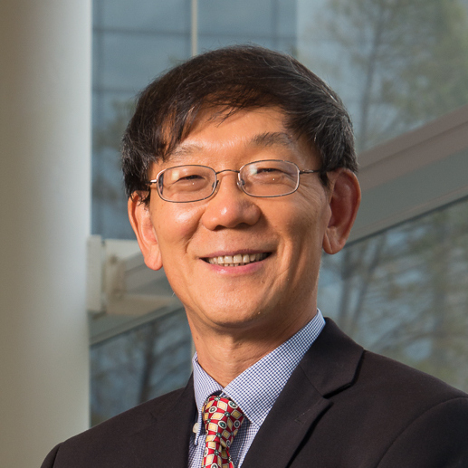 Kevin Zhang SVP Business Development |
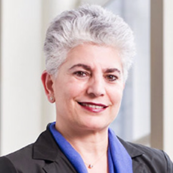 Maria Marced President, TSMC EU |
 Ian Cutress AnandTech |
Dr. Kevin Zhang has been TSMC’s Senior Vice President of Business Development for almost a year, having being promoted from the Design Technology Team. Previous to joining TSMC, Dr. Zhang spent 11 years at Intel as an Intel Fellow, becoming Vice President of the Technology and Manufacturing Group as well as Director of Circuit Technology. Dr. Zhang has published over 80 papers in technical conferences and research journals, holds 55 patents in integrated circuit technology, and holds a PhD in Electrical Engineering. Dr. Zhang will be the conference chair for ISSCC 2022.
Dr. Maria Marced is President of TSMC Europe, responsible for driving strategy and development of the company in the region, and has been in the position since 2007. Prior to this, Dr. Marced spent four years at NXP and 19 years at Intel in similar top-position roles. Dr. Marced serves as the Chairwoman of the EMEA Leadership Council of the GSA (Global Semiconductor Alliance), is on the board of CEVA, and holds a PhD in Telecommunications Engineering.
TSMC on The Leading Edge
Ian Cutress: TSMC has stated that it has had in-house EUV pellicle production since 2019, and TSMC is now vastly ramping up production of pellicles. How extensive is the use in manufacturing, and how does it further TSMC’s competitive advantage versus other fabs?
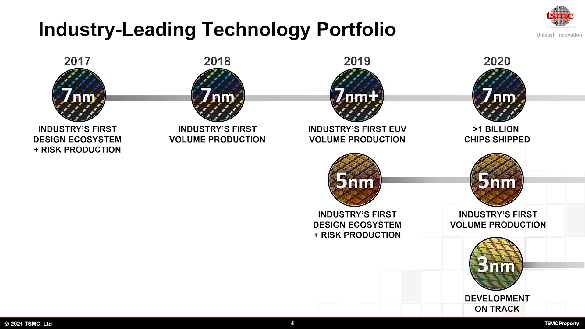
Kevin Zhang: We clearly have invested in this area in-house, and I think it is a very unique technology for us. We are able to leverage it to bring up our EUV mass production. If you look at the way we ran our 7 nm, on the 6 nm, and now in 5 nm, all with the EUV, clearly we have made tremendous progress. So this is definitely an area we think we have done well with our unique technology advantage.
Maria Marced: One thing, because I am here in Amsterdam, so we are relatively close to ASML - we have had special training by them. I can tell you, having this production in-house really allows us to extend the life of the masks. Typically in EUV, the mask gets dirty, and therefore, with short deadlines, this really helps us a lot to improve the productivity of EUV and the masks.
IC: So by having it on site means you’ve got less travel for the masks, and it gets less dirty due to less travel?
MM: That’s correct.

IC: We typically associate complex and specialty technologies with leading edge customers. Given that these customers are often in the low single digits, how does TSMC balance what packaging technologies to develop that customers need, compared to developing and pathfinding new technologies?
KZ: At the leading node, for example, we have been a leader - a technology leader. We want to continue to drive advancement of silicon technology, and we partner with our lead customers to optimize our technology. So this is definitely an area we continue to drive the future growth. But with that being said, I still think specialty technology also plays a very important role in our overall technology offering to our customers. Many of our customers can’t ship a single chip based on let's say, 5 nm, without maybe a 20 nm companion chip. If you look at a phone for example, there are multiple chips, and many companion chips. It is the same thing with automotive - you have an advanced chip there, but you also need a lot of microcontrollers based on mature technology.
So I think we have been doing a good job in balancing our overall technology development effort. We have invested in mature technology substantially over the past decades. If you look at our overall technology roadmap, we are providing the most advanced specialty technology offering today in the marketplace. I think Maria maybe will add some color from a Europe perspective.
MM: The only thing I will add is that it is very important for us to understand the system complexity of our customers. Also, especially by having these technologies that complete the bill of materials of the whole system, it helps us to better understand how the system architectures are evolving, and therefore do a better job for our customers.
IC: So how much of that goes down to what customers are specifically demanding, versus researching new technologies that customers don't know they need yet?
KZ: We have a separate team, for example, from an organization point of view. We have a separate team, a research team looking at things beyond the next generation. We really look far out for that to explore different things. It also requires lots of market input, and customer input. to help guide some of the exploratory work. So this is a pretty dynamic process, very interactive between us, within us, and between us and the customers.
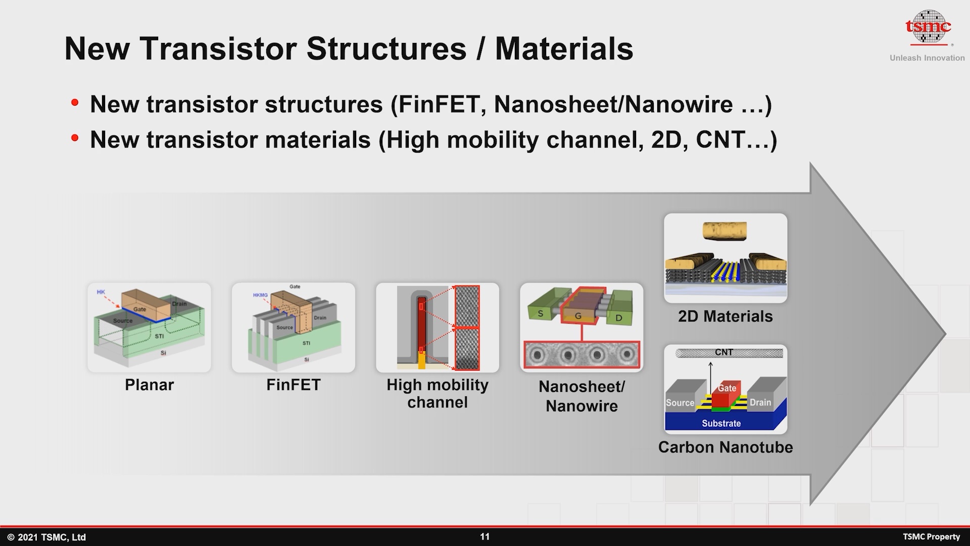
IC: TSMC has been very clear in saying that it is staying with FinFET, down to 3 nm, and moving to Gate-All-Around at 2 nm. By contrast, the competition is moving to GAA at an earlier stage of development. Can you describe how TSMC is weighing both its desire to be on the leading edge of these advanced technologies, but also maintaining the same FinFET for its production lines?
KZ: The reason we chose FinFET technology as a 3 nm is based on two things.
One, we have to figure out a way to improve the technology into more power efficiency, more performance, and the internal density. In the end the customer doesn't care whether it is FinFET, or Nanosheet. They want to look at it from their product point of view - about what kind of power, performance, and density benefit it can bring to the customer. That's the most important thing in the end. So we look at our FinFET technology, and we look at our innovation capability, we find a very very powerful knob, an innovative knob, that allows us to extend the FinFET technology down to 3 nm while also achieving substantial full node scaling benefits. So that's reason number one.
Reason number two is also the schedule. We want to make sure, at the right given time, we are able to deliver the most advanced technology. So predictability, from an advanced technology development point of view, is very very important. Our customers take scheduling very seriously! So combining the two, we made a decision to stay with the FinFET at 3nm. We believe in the 2022-2023 timeframe, our 3 nm will bring the most advanced logic technology to the marketplace.
IC: How do you balance pushing process density versus design complexity, such as 1D versus 2D metal routing? What are the current possibilities on leading nodes?
KZ: We look at all the different metrics. At the end of the day, we consider really what it is at a product level, at a system level, and what kind of overall scaling benefit we can bring the customer. When I talk about the scaling benefits, I refer to overall power/performance and the costs. This has to be done at the system level, it's not simply at the chip level.
In the past, two dimensional scaling dominated everything, but now we have to look more at a system level. For example, you notice that we spend a lot of effort and investment developing chip level integration schemes: we have 2D, 2.5D, and 3D going forward. This all comes into play to basically provide a complete system level solution for the future. I think you will see more and more applications based on sophisticated advanced chip level integration technology. Transistor development continues to be important, make no mistake, and this will continue to be very very important. Providing the customer the best energy efficient transistors is still very very important, but that's not going to be sufficient.
We look at overall scaling at the system level. So lots of co-optimization between technology, different aspects of the technology, and the product system level design.
IC: As process nodes shrink, resistance on metal layers is becoming more problematic. With regards innovative solutions, and exotic materials versus copper interconnects, is it just a case of more research down that front? Or do we need to put more effort into increasing and routing higher metal layers?
KZ: I think in the research session at our advanced technology introduction, we did cover a little bit about the back end work. For example, we are continuing to optimize the copper grain boundary to bring a lower resistance metal line to our overall chip technology and new technology. Also, with dielectrics we continue to find innovative materials to improve the dielectric in parasitic capacitance. So, those things are being actively researched.
The 3D integration can also bring an alternative solution to this whole performance requirement in the back-end. You can instead route from A to B in a 2 dimensional space, or you can route A to B vertically in 3 dimensions. In some cases, by going vertical, you can reduce the overall length of the RC wire, and reduce pass delay significantly. So all those things have to be looked at going forward.
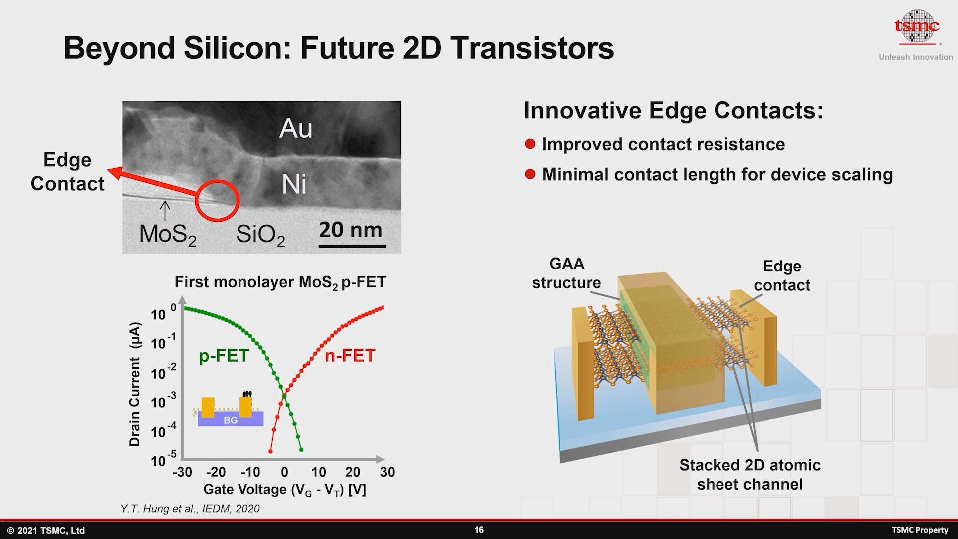
IC: So looking into new technologies, the two most promising technologies as we go beyond Gate-All-Around are 2D transistors and carbon nanotubes. TSMC recently launched a paper that got a lot of press regarding new developments on 2D transistors. Can you comment on what looks more promising?
KZ: All those advanced materials for transistors have certain advantages. That's why we spend early R&D efforts to explore those, but those are still pretty far out. There are a lot of things that still need to be better understood, especially as it will take tremendous effort to bring those kinds of new materials, and new structures, into a large-scale manufacturing base. So there is still a lot of work ahead of us. But the good thing is we are not lacking in new ideas. There are lots of new things we're exploring, and they all have a certain advantage. So we just need to figure out how to integrate them all together to bring out the most compelling overall technology solution to our future customers' applications.
IC: Regarding the research in collaboration with ASML, they've spoken about future EUV developments such as high NA (numerical aperture) optics. They keep talking to us about it! But as an extension of that, can you speak about what TSMC is necessarily doing regarding post-EUV technologies?
KZ: We look at all different technology options. We talked a little bit at the conference about material innovations to bring new materials integrated on the silicon to allow us to achieve better conduction and a more power efficient transistor. Those are important areas in which we have a research team and an early R&D team to develop and explore all different options.
On lithography, obviously it continues to be a very important part in scaling the geometry. So we do have a team also looking into how to maximize EUV, to print even tighter pitches going forward. All those things are being explored for the future of technology options.
Going Beyond Asia
IC: With regards to these most advanced technologies, and leading edge capabilities, for Europe we've heard that the competitors of TSMC are investing in their European facilities. We've not necessarily heard the same from TSMC. Is there a particular reason for this? Or is there something that is to be announced?
MM: Well, we wouldn’t rule out anything. However, today, I do not have any details to share with you!
IC: On your European customers - only a few of them are kind of on the leading edge? Most of them rely on the older process technologies, specialty technologies - such as the big automotive industry in Germany. We don't necessarily see that there's a lot of desire to go leading edge from European business. Can you comment?
MM: The main segments in Europe are automotive, industrial, but also where Europe is very important as well is in the Internet of Things (IoT). The technologies that are required by those segments are more on the specialty side, and more on the advanced, not only mature, but advanced technologies.
IC: We're obviously seeing a lot of semiconductor demand for AI. Lots of customers want leading edge solutions, but there is also lots of demand for edge products on the more mature nodes. Can you talk to developments on how demand is shifting when it comes to AI, and perhaps a mention of the EU given that China and North America gets the spotlight?
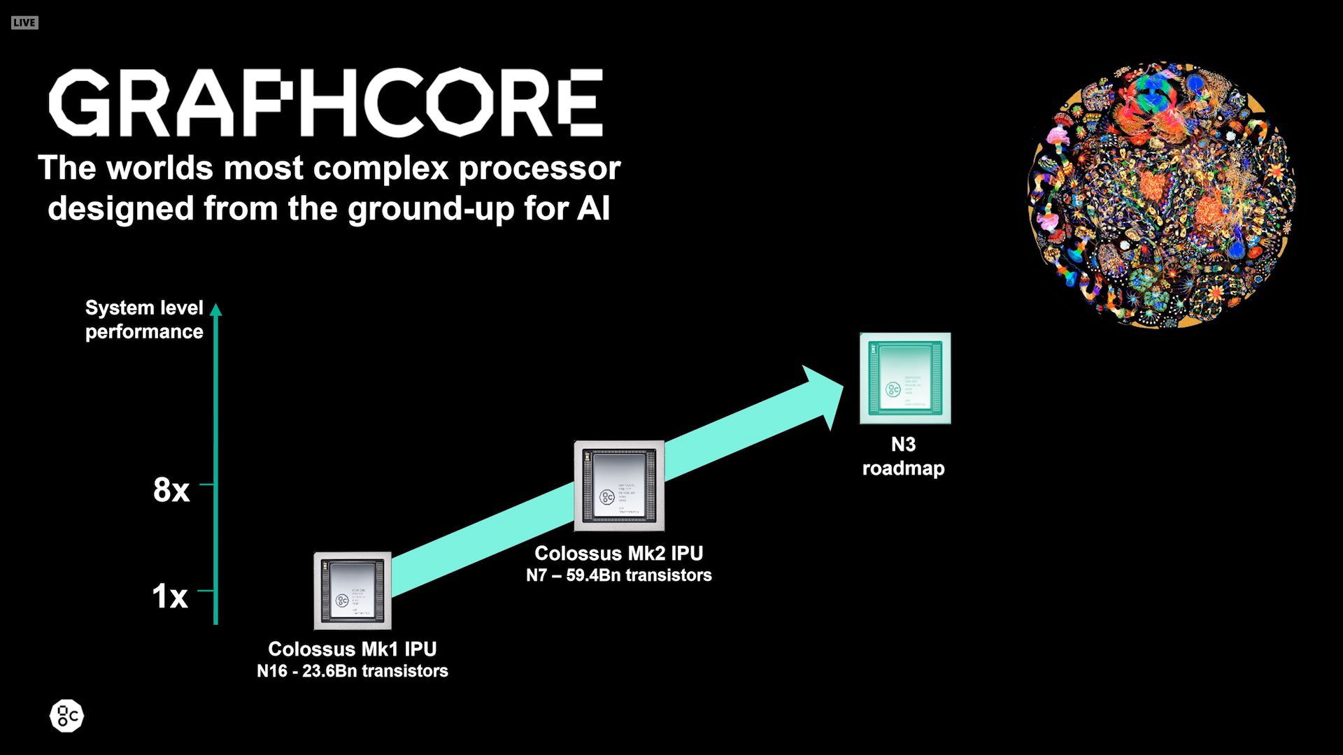
MM: Well, even in the UK, you have good AI companies! You know that one of them is one of our early adopter customers in several initiatives (Ian: Graphcore already announced working with TSMC at 3nm). But also in Israel, we see a lot of activity around AI. So in EMEA we see a lot of interest in artificial intelligence, and even the EU has some activity leaning towards what they call the European Processor Initiative (EPI), which revolves around the use of artificial intelligence.
So yes, we see a lot of activity. Actually, today, I was very proud that during my presentation at the conference, I got an email from Matteo Vallejo from the University in Barcelona, which is very much involved in AI. So of course, China and the US are always very advanced in high performance computing, but we also see a lot of interest in Europe, and a lot of VC money in AI.
IC: TSMC likes to promote where the revenue is coming from, and the proportion of revenue it receives from North America seems to be increasing, at the expense of the proportion from Europe. Are there any headwinds or tailwinds about Europe that we should think about?
MM: The main reason I think is that because Europe’s main segments are automotive, industrial, and IoT. Those segments are still using mature advanced technologies, and specialty technologies, and a lot of these end-products have a lower ASP, and this creates a big difference in terms of the percentage of revenues. How is this moving forward? Fast, because automotive, as well as industrial, especially as part of industry 4.0 and IoT, are because AI offerings are moving fast towards more advanced, more leading edge technology. So I really expect that this proportion is going to change significantly in the future.
IC: TSMC has three main geographical regions - TSMC Asia, TSMC North America, and TSMC EMEA. How much are these independent organization from each other - how much collaboration occurs? Is it right to be split, given that companies often work worldwide or in multiple markets?
MM: Oh this is an interesting question! I really believe in companies being centralized, having worked at Intel for many years (Maria was at Intel for 19 years), I really believe in companies being centralized and having one direction coming from the leadership of the company. So we are not independent organizations at all! We are very dependent on each other, and I can tell you I usually spend most of my time traveling to Taiwan - now video conferencing with Taiwan. But absolutely we have one direction, and we complement each other very well. I think Europe is bringing something different, which is focused more on and around specialties. This is where we play the key role. We are really one company with one direction.
Building and Expanding
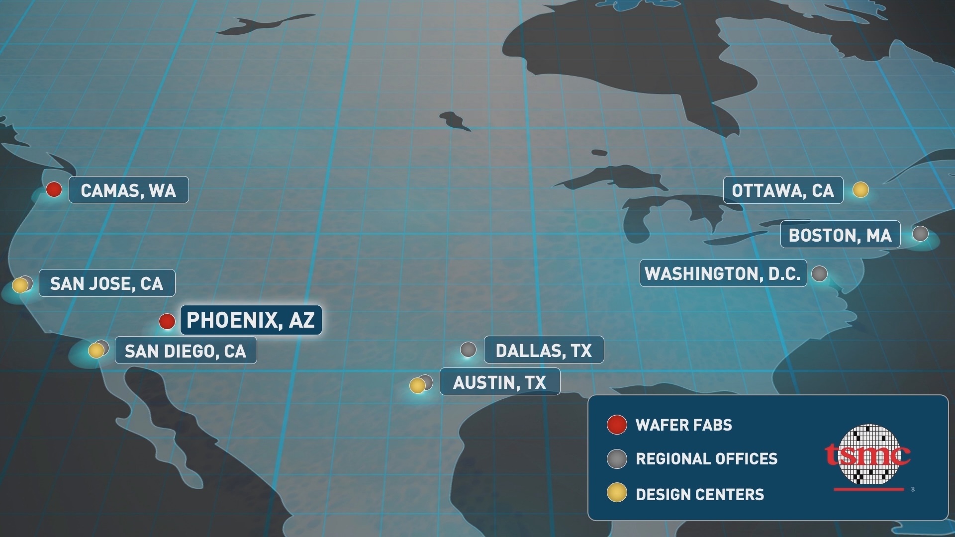
IC: Pivoting to packaging, the CEO mentioned that there are five fabs enabling SoIC and a new fab in Chunan with more capacity. Normally we measure production fabs in wafers per month, so how should we consider the throughput of these new SoIC facilities?
KZ: I can't give you a specific capacity number, but all that I can say is that we're really investing in our backend capability and capacities. This is because we do see a trend that more and more customers want to leverage our advanced packaging options, including CoWoS, InFO, and going forward, SoIC with 3D integration. So that's why we're investing not only in the R&D side, but we're also investing in the capacity side to prepare for future growth.
With 3D packaging capacity metrics, it depends on what kind of configuration you do. Sometimes you could potentially do a very advanced chiplet integrated with more mature nodes, and minus one or minus two nodes, so that you probably have to compute the total volume differently. It all depends on the specific product configuration. Maybe in the future, we'll have to figure out a way to better measure the volume and report the numbers. For the definition volume, when you come to 3D integration, it may be that we count the number of final integrated parts.
IC: TSMC currently has four packaging facilities, and this fifth one (called AP6) is being built in Chunan. AP6 would have over 50% of the packaging capacity of TSMC globally. Are there any positive or negative implications for having a large portion of all TSMC’s packaging in one area?
KZ: We do a lot of balancing - there's an advantage for us by building a larger scale manufacturing facility. I think you probably already know that we build Gigafabs today with large scales. I think that that's a key economic benefit that we can bring to our customers, enabling lower costs that will also be passed on to the customer. But we do have to have considerations on how to spread that to different locations. We are doing that, making sure we maintain a certain balance. In a similar light, we are building a factory in Arizona pretty far away from Taiwan!
IC: Speaking about packaging and OSAT bottlenecks. When speaking with our audience, a number of them seem to think it is wafer throughput, and some of them believe it comes down to packaging throughput. I don't necessarily want to ask you about which one is the most bottlenecked but I do want to ask about how TSMC is improving throughput of customer orders. We’ve spoken about TSMC expanding its packaging, but is there anything TSMC can do here?
KZ: I think on the technical part, your readers want to view it as either the wafer technology is the bottleneck, or the packaging technologies are the bottleneck. Actually the way I look at it is how we are finding the optimum solution to bring all the pieces together at a system level to provide the best result. If you look back at semiconductor technology, it started with two dimensional things, and Moore's law is about the transistor density, scaling, and economics. But now as we're moving forward, I see the whole industry trending as we move towards a higher level of integration. In technical conferences, such as ISSCC, you see people not only talk about transistor level design, but they also talk about system level performance, and how to bring all of the functions and all the pieces together. In the future, I think that this trend will continue, so it's really about working with your customers for their given product application, given their unique system level requirements, and how you bring all of the pieces together in an optimum fashion. This is how I look at it in the future.
MM: Our key thing is that we collaborate to innovate. Collaborating with our customers is our best way to really innovate, allowing their innovations and at the same time boosting our own innovations.
IC: DTCO (Design Technology Co-Optimization) is an integral part of making most out of leading edge technologies. Is DTCO getting more complex, or as TSMC and its customers understand the process behind achieving good DTCO, is it accelerating? Can you talk about that?
KZ: I think our customers have benefited greatly from design technology co-optimization over the last couple of generations. Going forward, there will be more DTCO to do, and we find our customers are more eager and willing to collaborate with us in order to harvest intrinsic technology benefits. I think this trend will continue and I think the effort even then will be stronger going forward. As they need to be more intertwined between technology and the design, you could call it harder? I think it will become more delicate, and we need to work closer with our customers to really optimize things together. Now you also have advanced packaging coming in, so how a system can partition its technology could vary. If you have a chiplet, how you architect it at a system level from the get-go, you need to think about how to architect your system in the right way by leveraging different pieces of silicon technology and different integration schemes.
Many thanks to Kevin, Maria, and TSMC's Comms teams for their time.
Also thanks to Gavin Bonshor for transcription.


17 Comments
View All Comments
Ian Cutress - Wednesday, June 9, 2021 - link
Every briefing I have with Andrew Feldman at Cerebras is 20 minutes of amusing banter and 10 minutes of 'oh right I still have to tell you about this new thing we're talking about'. He's a great laugh :). When we all get flying again, I've an open invitation to go by their Santa Clara offices, so it might be worth waiting until later in the year when I can get hands on with a WSE2 and we can do an interview in person, between myself, Andrew, and Natalia Vassilieva.Slash3 - Wednesday, June 9, 2021 - link
Sounds like a great time and a great plan, and I'll look forward to it hopefully happening! We've got plenty to occupy ourselves with in the interim this year for tech news and reviews, but those WSEs are so far outside of the norm that reading anything about them is a guaranteed treat.six_tymes - Wednesday, June 9, 2021 - link
they act as if they were first to use FinFet. a smug remarkzodiacfml - Wednesday, June 9, 2021 - link
nothing surprising but at least cements some ideas out there. we also have to consider Apple and AMD as one of their largest customers, controlling or having input to TSMCs direction especially on packaging/integration.garaldas - Sunday, June 13, 2021 - link
" Frederick Chen
Advanced Memory Development at Winbond Electronics
They previously chose differently:
https://esg.tsmc.com/csr/en/update/greenManufactur...
"TSMC has chosen EUV mask without pellicle to enhance optical transmittance, thus reducing energy loss during exposure process." "
https://www.linkedin.com/feed/update/urn:li:activi...
Fataliity - Monday, June 14, 2021 - link
That's just wrong. They likely did this to put off their competitors.They announcted in October of 2019 earnings that they had their own pellicle and produce their own pellicle. Everything else was just smoke and mirrors.
garaldas - Wednesday, June 16, 2021 - link
https://esg.tsmc.com/csr/en/update/greenManufactur...
THEN WHAT ABOUT THE STATEMENT IN THE THIRD TAB IN THE TOP GRAPHICS.