Arm Announces Mobile Armv9 CPU Microarchitectures: Cortex-X2, Cortex-A710 & Cortex-A510
by Andrei Frumusanu on May 25, 2021 9:00 AM EST- Posted in
- SoCs
- CPUs
- Arm
- Smartphones
- Mobile
- Cortex
- ARMv9
- Cortex-X2
- Cortex-A710
- Cortex-A510
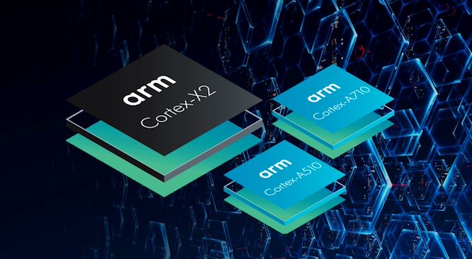
It’s that time of the year again, and after last month’s unveiling of Arm’s newest infrastructure Neoverse V1 and Neoverse N2 CPU IPs, it’s now time to cover the client and mobile side of things. This year, things Arm is shaking things up quite a bit more than usual as we’re seeing three new generation microarchitectures for mobile and client: The flagship Cortex-X2 core, a new A78 successor in the form of the Cortex-A710, and for the first time in years, a brand-new little core with the new Cortex-A510. The three new CPUs form a new trio of Armv9 compatible designs that aim to mark a larger architectural/ISA shift that comes very seldomly in the industry.
Alongside the new CPU cores, we’re also seeing a new L3 and cluster design with the DSU-110, and Arm is also making a big upgrade in its interconnect IP with the new cache coherent CI-700 mesh network and NI-700 network-on-chip IPs.
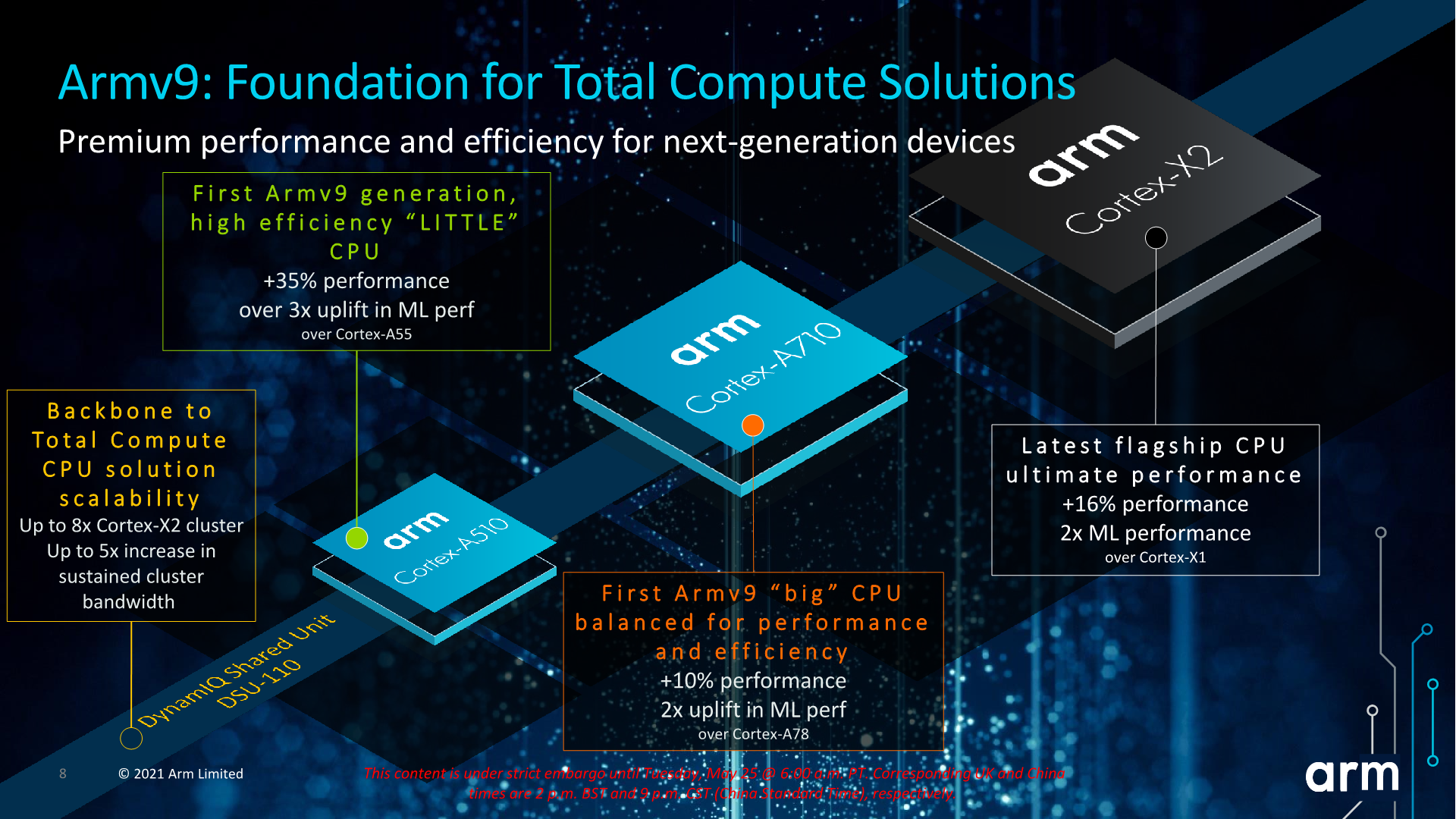
The Cortex-X2, A710 and A510 follow up on last year's X1, A78 and A55. For the new Cortex-X2 and A710 in particular, these are direct microarchitectural successors to their predecessors. These parts, while iterating on generational improvements in IPC and efficiency, also incorporate brand-new architectural features in the form of Armv9 and new extensions such as SVE2.
The Cortex-A510, Arm's new little core, is a larger microarchitectural jump, as it represents a new clean-sheet CPU design from Arm’s Cambridge CPU design team. A510 brings large IPC improvements while still having a continued focus on power efficiency, and, perhaps most interestingly, retains its characteristic in-order microarchitectural.
An Armv9 CPU Family – AArch64 only for all practical purposes*
The new CPU family marks one of the largest architectural jumps we’ve had in years, as the company is now baselining all three new CPU IPs on Armv9.0. We've extensively covered the details of the new Arm architecture back in late March. Cornerstone features of the new ISA include the new enrollment of prior optional/missing Armv8.2+ features that weren’t guaranteed in mobile and client designs (mostly due to the older A55 cores), and the introduction of new SVE2 SIMD and vector extensions.
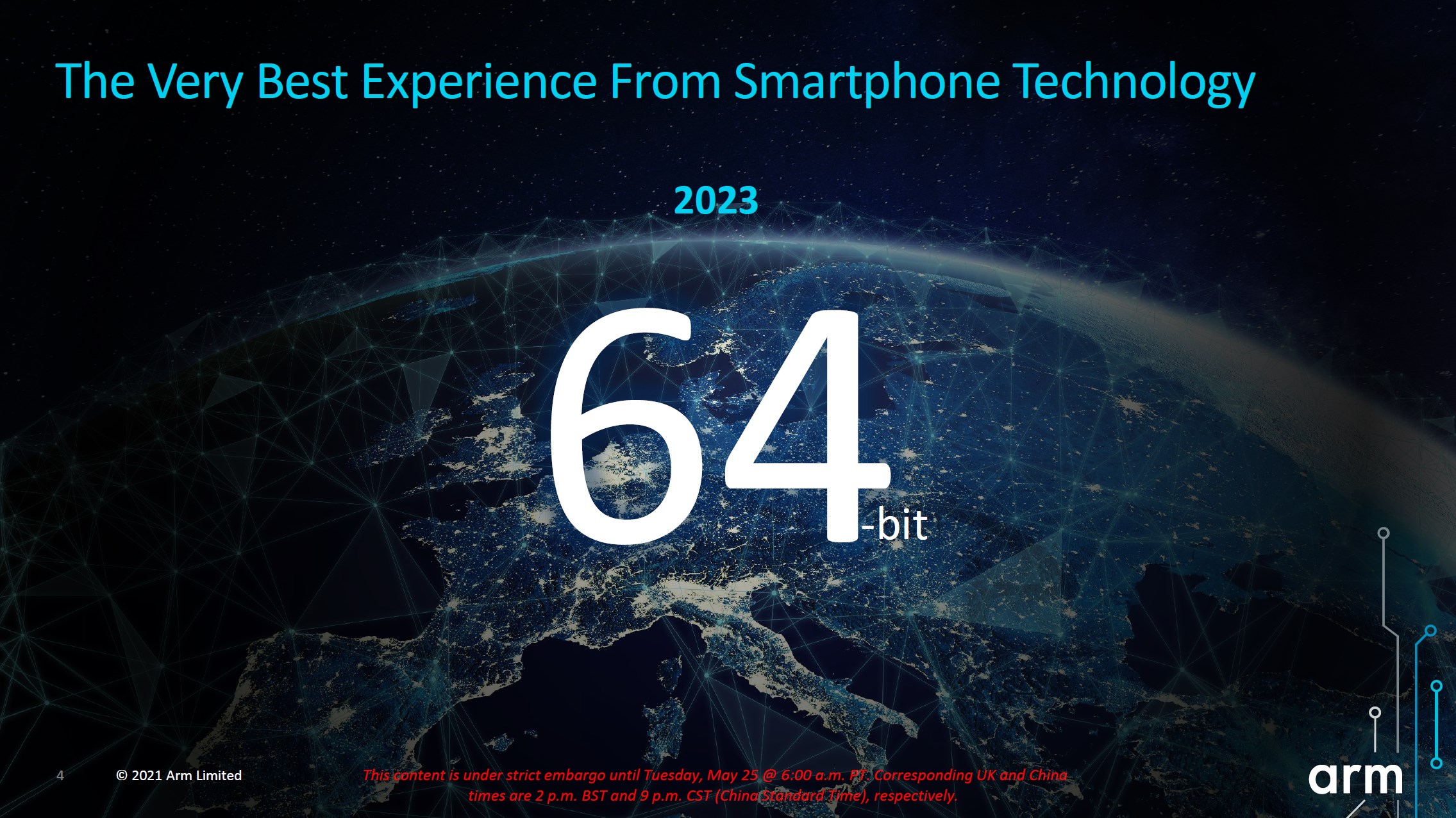
One big change we’ve been expecting for quite some time now is that we’ll be seeing a deprecation of the 32-bit AArch32 execution mode in upcoming Arm Cortex-A mobile cores. The clock has been ticking for 32-bit apps ever since Google’s announced in 2019 that the Google Play store will require for 64-bit app uploads, and the company will stop serving 32-bit applications to 64-bit compatible devices later this summer
While Arm is declaring that shift to happen in 2023, for all intents and purposes it’s already happening next year for most global users. Both the Cortex-X2 flagship core and the Cortex-A510 little cores are AArch64-only microarchitectures that are no longer able to execute AArch32 code.
With that said, sharp readers will note that two out of three CPUs isn't a complete shift, and the reason for that is because the Cortex-A710 actually still supports AArch32. Arm states that the reason for this is primarily to meet the needs of the Chinese mobile market, which lacks the homogeneous ecosystem capabilities of the global Play Store markets, and Chinese vendors and their domestic app market require a little more time to facilitate the shift towards 64-bit only. This means we’ll have an odd scenario next year of having SoCs on which only the middle cores are able to execute 32-bit applications, with those apps being relegated to the middle A710 cores and missing out on the little A510 cores’ power efficiency or the X2 cores’ performance.
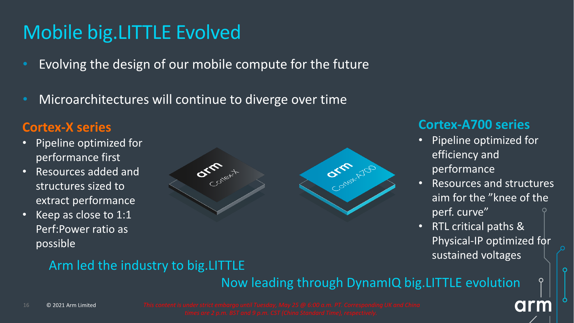
On the big core side, the new Cortex-X2 and Cortex-A710 are successors to the Cortex-X1 and Cortex-A78. Both designs are mostly designed by Arm’s Austin design team, and represent the 4th generation of this microarchitecture family, which had started off with the Cortex-A76 several years ago. These cores should be the last of this microarchitecture family before Arm hands things off to a completely new design with next year’s new Sophia cores.
In terms of design philosophy, the X2 and A710 generally keep the same overarching goals the X1 and A78 had defined: The X-series continues to focus on advancing performance by increasing microarchitectural structures and by Arm being willing to make compromises on power within reasonable limits. Meanwhile the A710 continues to focus on advancing performance and efficiency through smarter design and with a large focus on maximizing the power, performance, and area (PPA) balance of the IP.
One point Arm makes in the above slide is having optimized critical paths and physical design for sustained voltage operations – this is more of a goal the company is striving for in the next generations of “middle” cores rather than something that’s specifically reflected in the Cortex-A710.
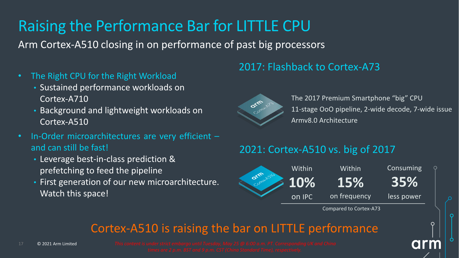
This year, we are also finally seeing a new little core. We had covered the Cortex-A55 back in 2017, and since then we haven’t had seen any updates to Arm’s little cores, to the point of it being seen as large weakness of last few generations of mobile SoCs.
The new Cortex-A510 is a clean-sheet design from Arm’s Cambridge design team, leveraging a lot of the technologies that had been employed in the company’s larger cores, but implemented into a new in-order little microarchitecture. Yes – we’re still talking about an in-order core, and Arm still sees this to be the best choice in terms of extracting the best efficiency and “Days of use” of mobile devices.
Even though it’s a in-order core, Arm made a comparison that the new design is extremely similar to a flagship core of 2017 – namely the Cortex-A73, achieving very similar IPC and frequency capabilities whilst consuming a lot less power.
The new design also comes with a very interesting shared complex approach and shares the L2 and FP/SIMD pipelines with a second core, a design approach Arm calls “merged core” and undoubtedly will remind readers of AMD’s CMT approach in Bulldozer cores 10 years ago, even though there are quite important differences in the approaches.


181 Comments
View All Comments
Ppietra - Tuesday, May 25, 2021 - link
I believe that he was talking about the overall SPEC2006 score and not just SPECint. Still he would be wrong about the X1 score, which would be 50 and not 40 (probably a typo).Anyway a 16% improvement for X2 over X1 would mean a score of 58 which, like he said, would still be behind the A13 performance core and well behind the 72 score for the A14.
X1 is already being manufactured at 5nm, so it makes no sense to factor in a transition from 7nm.
Wilco1 - Tuesday, May 25, 2021 - link
Cortex-X1 can reach 3.2GHz in Samsung's 5nm process but the power is too high: https://images.anandtech.com/doci/16463/2100-volta...TSMC 5nm is faster and lower power, which allows for higher frequencies. At a conservative 3.3GHz X2 would have a combined score of ~66.7 (only 7% slower than A14).
Ppietra - Tuesday, May 25, 2021 - link
That is not how it works!First of all you have no idea what would be the advantage from using TSMC instead of Samsung, so you are just throwing numbers with no substance. Secondly, X1 energy consumption is already very high (it is less efficient than the A14 Firestorm core), so no, there doesn’t seem to be a lot of room to improve X2 clock speed to 3.3GHz. Thirdly even with your assumption you would still have X2 performing worse than a 1 year old core
Wilco1 - Tuesday, May 25, 2021 - link
We absolutely do know. TSMC 5nm is ~15% faster than 7nm at the same power (or 30% lower power at the same frequency). We know that SD865+ achieves 3.1GHz on 7nm and that the frequency gain from A13 on 7nm to A14 on 5nm was around 13%. So 3.3GHz should be feasible on 5nm without increasing power.The point is that TSMC 5nm will give a significant perf/power boost (that A14 already benefits from). And that means the gap has narrowed to only one generation rather than 2.
melgross - Tuesday, May 25, 2021 - link
It’s not that simple. The cores would require a bit of a redesign for the different process, and each design would fare differently. Some might get a good boost, and others may not.michael2k - Tuesday, May 25, 2021 - link
You're comparing the X2 to the A14? I mean, if we're lucky we will see the X2 in 2022 alongside the A16. The A15 will be released this year, in 2021. We already have some X1 baselines:https://www.anandtech.com/show/16463/snapdragon-88...
So in terms of generation:
2021 X1 not competitive with the 2019 A13 now
2021 X1 competitive with the 2019 A13 on TSMC 5nm
2021 X1 not competitive with the 2021 A15 (est 10% boost to hit 70 SPECint)
2022 X2 competitive with the 2020 A14 on TSMC 5nm
2022 X2 not competitive with the 2021 A15
That still sounds like a 2 generation gap to me. The real problem isn't fundamentally the core, but the OEM choosing not to use a 2x2 design (2 X1 and 2 A77) or (2 X2 and 2 A710), so even if the cores get faster each generation, overall performance is hobbled by using 3 medium cores instead of a pair of higher performance X1 or X2 cores.
Fulljack - Wednesday, May 26, 2021 - link
it's cat and mouse, really. Apple release their phones in late Q3, while Samsung S-series are released in late Q1. there's 5 to 6 month difference.Ppietra - Wednesday, May 26, 2021 - link
Nothing of what you said gives you any data to infer about a transition from Samsung to TSMC.SD865+ does not use a X1 core, as such you have no commonality to make that kind jump in analysis, secondly the X1 core already consumes significantly more than the SD865+ core, so clearly there is no much room to increase clock speed from that perspective. If you want to increase clock speed you need to keep power consumption under control.
Wilco1 - Wednesday, May 26, 2021 - link
These are different generations of the same microarchitecture from the same design team with the same frequency capability (as reported by AnandTech). So yes there is obvious commonality.We also know this microarchitecture is capable of higher frequencies, for example AnandTech reports Cortex-X1 can reach 3.2GHz. The main problem is power however, which is what limited Cortex-X1 on Samsung's process. TSMC 5nm reduces power by 30% which enables higher clock speeds.
Ppietra - Wednesday, May 26, 2021 - link
actually they aren’t different generations from the same microarchitecture. The next generation for the A77 is the A78. The X1 goes for a bigger core design, and as such consumes more.Being capable of higher frequencies doesn't mean that Qualcomm (, etc) finds it viable to use those higher frequencies in a smartphone SoC...
NODE power reduction is stated for same performance and microarchitecture (which X1 is not) and only as an internal TSMC comparison... The data you give tells you nothing about X1 (already at 5nm) transitioning to TSMC. You are making an analysis based on wrong assumptions.