The Ampere Altra Review: 2x 80 Cores Arm Server Performance Monster
by Andrei Frumusanu on December 18, 2020 6:00 AM EST- Posted in
- Servers
- Neoverse N1
- Ampere
- Altra
As we’re wrapping up 2020, one last large review item for the year is Ampere’s long promised new Altra Arm server processor. This year has indeed been the year where Arm servers have had a breakthrough; Arm’s new Neoverse-N1 CPU core had been the IP designer’s first true dedicated server core, promising focused performance and efficiency for the datacentre.
Earlier in the year we had the chance to test out the first Neoverse-N1 silicon in the form of Amazon’s Graviton2 inside of AWS EC2 cloud compute offering. The Graviton2 seemed like a very impressive design, but was rather conservative in its goals, and it’s also a piece of hardware that the general public cannot access outside of Amazon’s own cloud services.
Ampere Computing, founded in 2017 by former Intel president Renée James, built upon initial IP and design talent of AppliedMicro’s X-Gene CPUs, and with Arm Holdings becoming an investor in 2019, is at this moment in time the sole “true” merchant silicon vendor designing and offering up Neoverse-N1 server designs.
To date, the company has had a few products out in the form of the eMAG chips, but with rather disappointing performance figures - understandable given that those were essentially legacy products based on the old X-Gene microarchitecture.
Ampere’s new Altra product line, on the other hand is the culmination of several years of work and close collaboration with Arm – and the company first “true” product which can be viewed as Ampere pedigree.
Today, with hardware in hand, we’re finally taking a look at the very first publicly available high-performance Neoverse based Arm server hardware, designed for nothing less than maximum achievable performance, aiming to battle the best designs from Intel and AMD.
Mount Jade Server with Altra Quicksilver
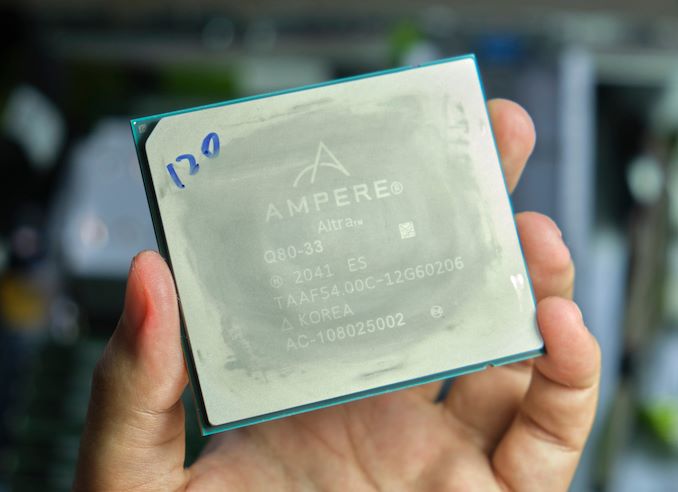
Ampere has supplied us with the company’s server reference design, dubbed “Mount Jade”, a 2-socket 2U rack unit sever. The server came supplied with two Altra Q80-33 processors, Ampere’s top-of-the-line SKU with each featuring 80 cores running at up to 3.3GHz, with TDP reaching up to 250W per socket.
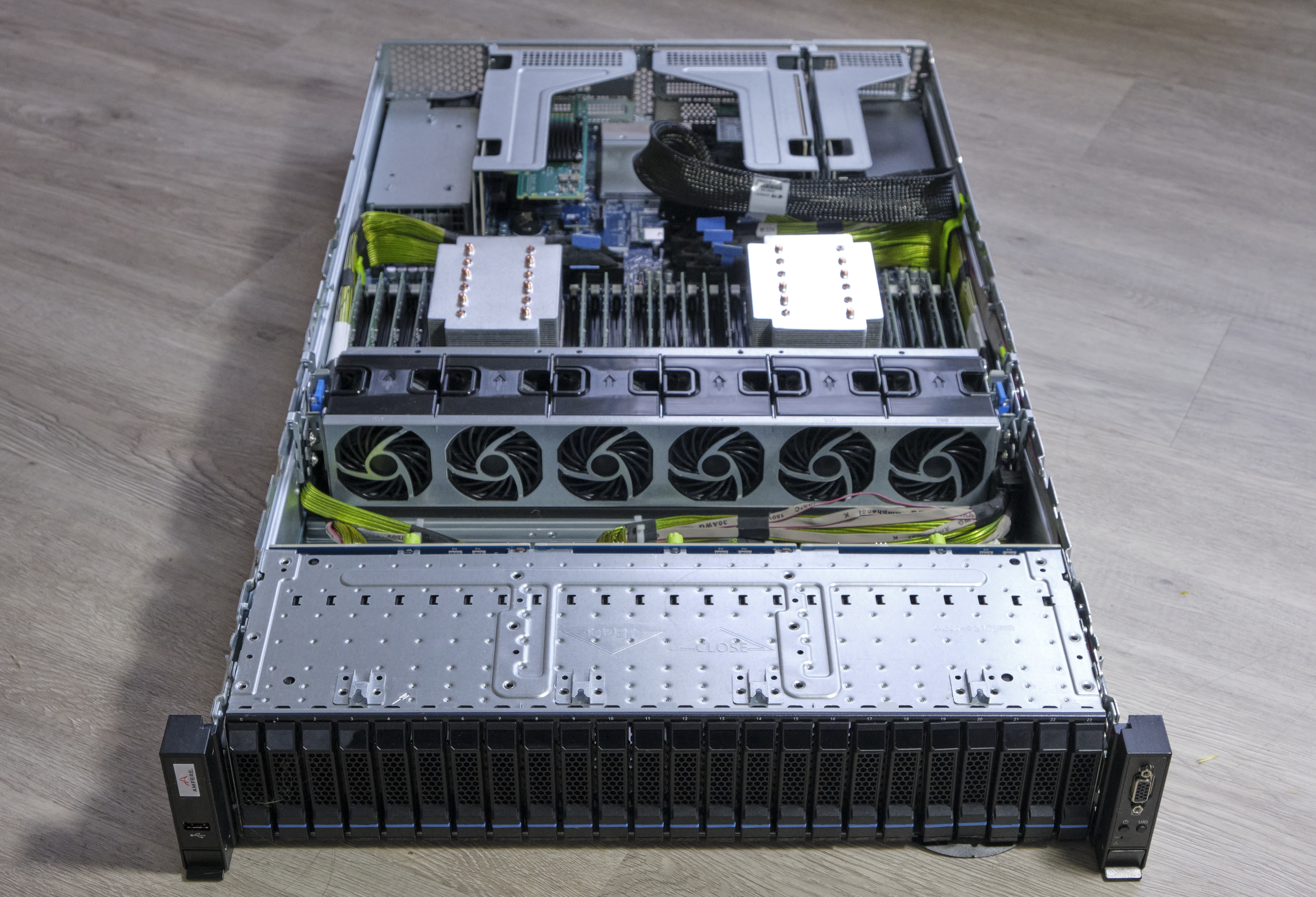
The server was designed with close collaboration with Wiwynn for this dual socket, and with GIGABYTE for the single socket variant, as previously hinted by the two company’s announcements of leading hyperscale deployments of the Altra platforms. The Ampere-branded Mount Jade DVT reference motherboard comes in a typical server blue colour scheme and features 2 sockets with up to 16 DIMM slots per socket, reaching up to 4TB DRAM capacity per socket, although our review unit came equipped with 256GB per socket across 8 DIMMs to fully populate the chip’s 8-channel memory controllers.
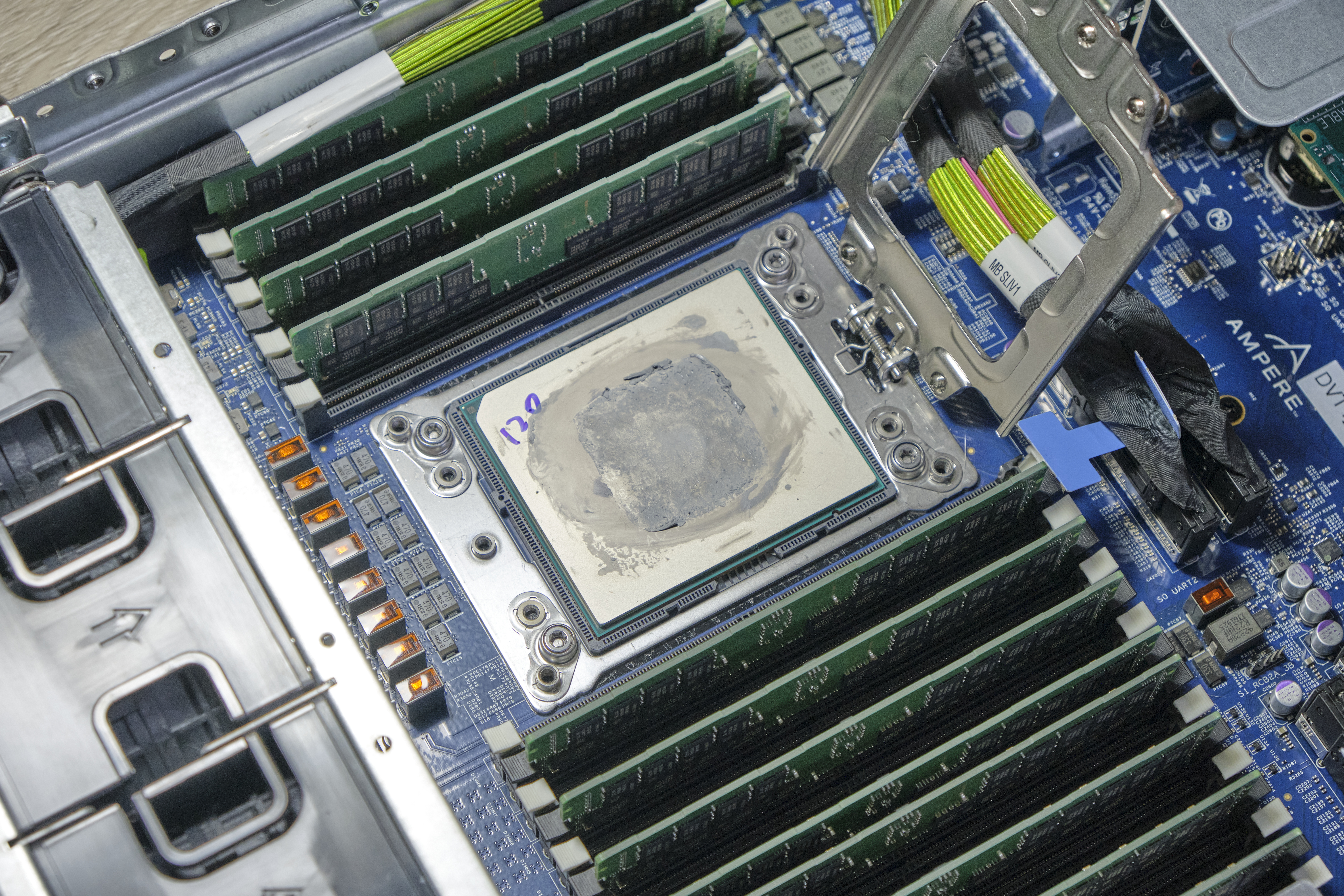
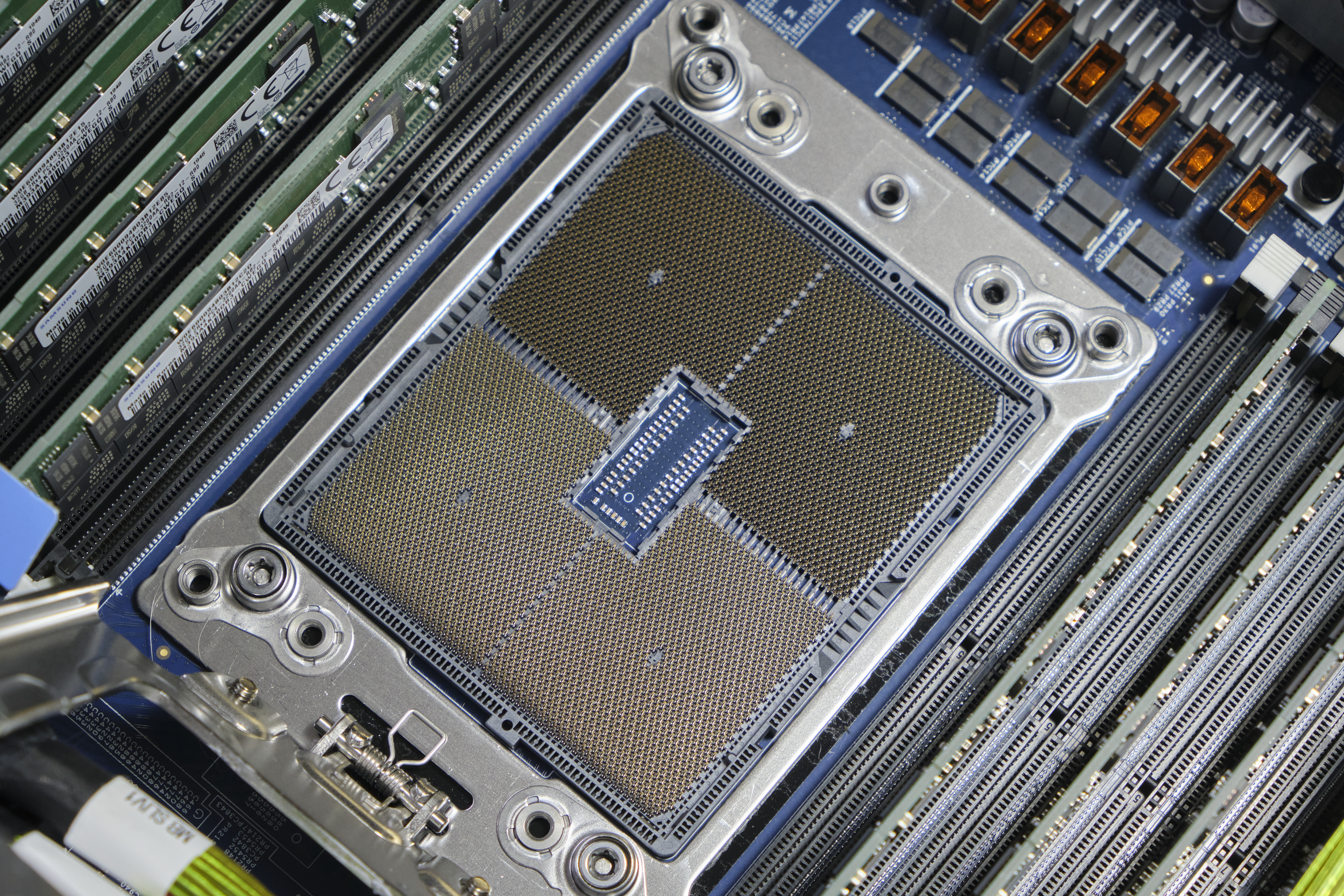
This is also our first look at Ampere’s first-generation socket design. The company doesn’t really market any particular name to the socket, but it’s a massive LGA4926 socket with a pin-count in excess of any other commercial server socket from AMD or Intel. The holding mechanism is somewhat similar to that of AMD’s SP3 system, with a holding mechanism tensioned by a 5-point screw system.
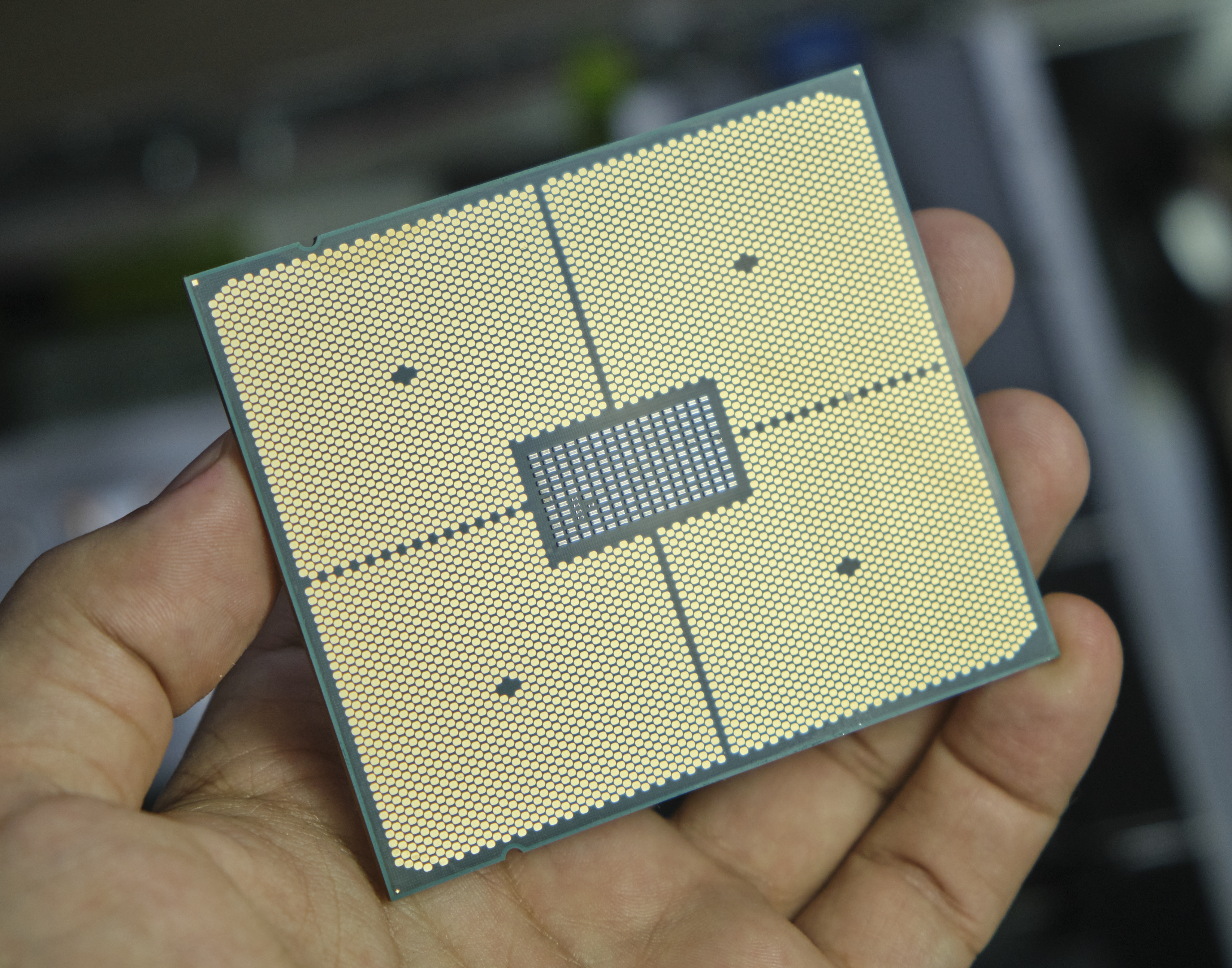
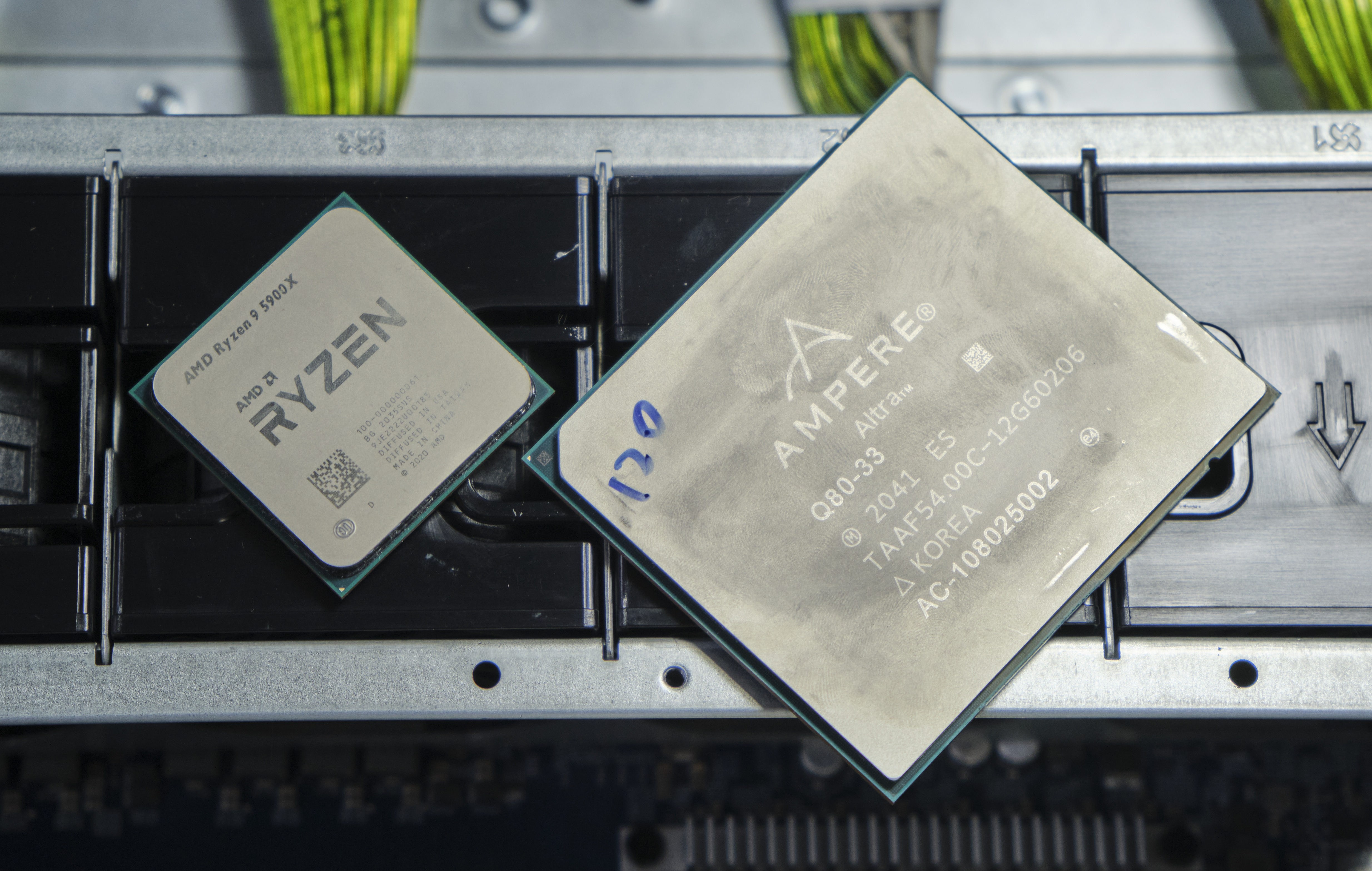
The chip itself is absolutely humongous and amongst the current publicly available processors is the biggest in the industry, out-sizing AMD’s SP3 form-factor packaging, coming in at around 77 x 66.8mm – about the same length but considerably wider than AMD’s counterparts.
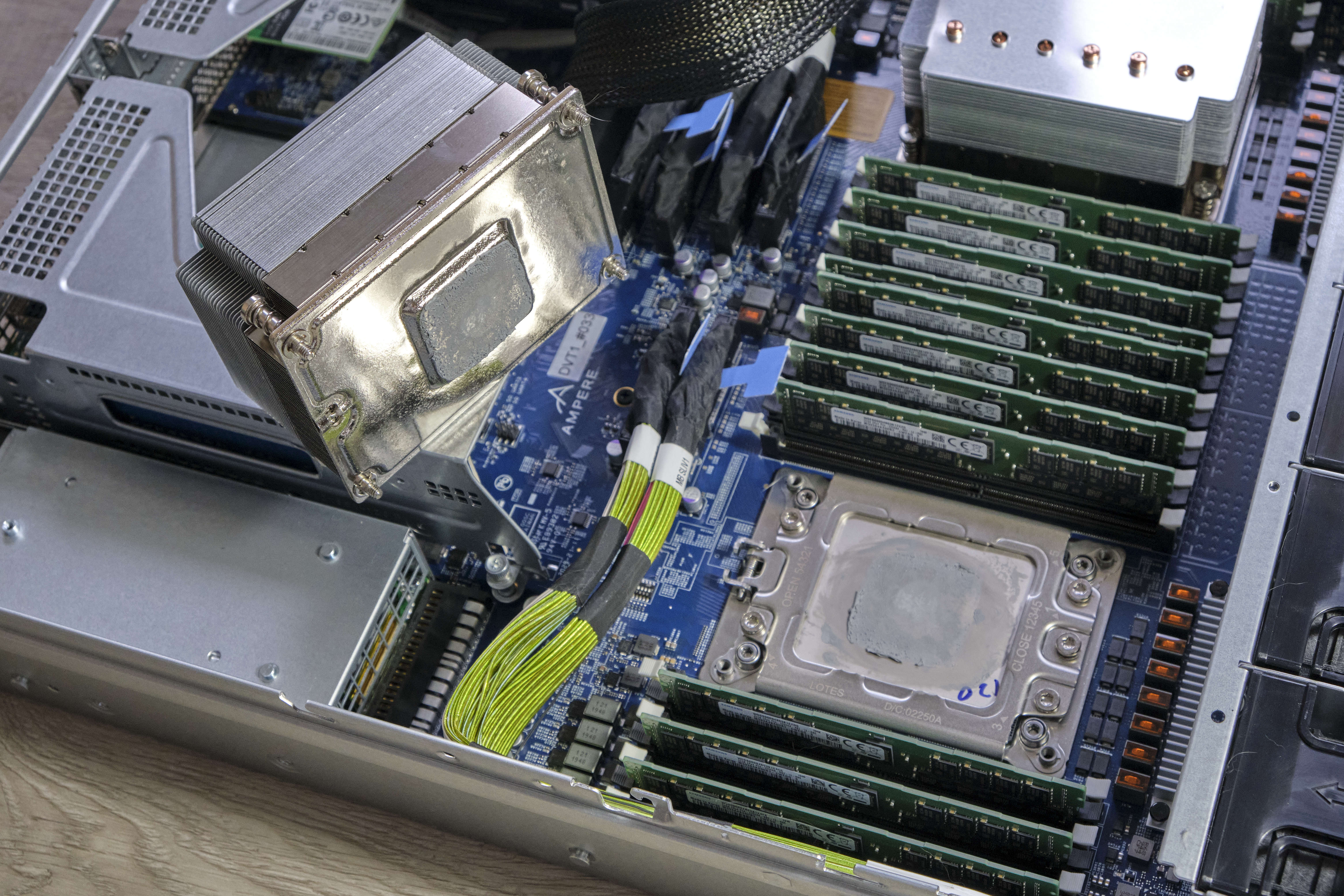
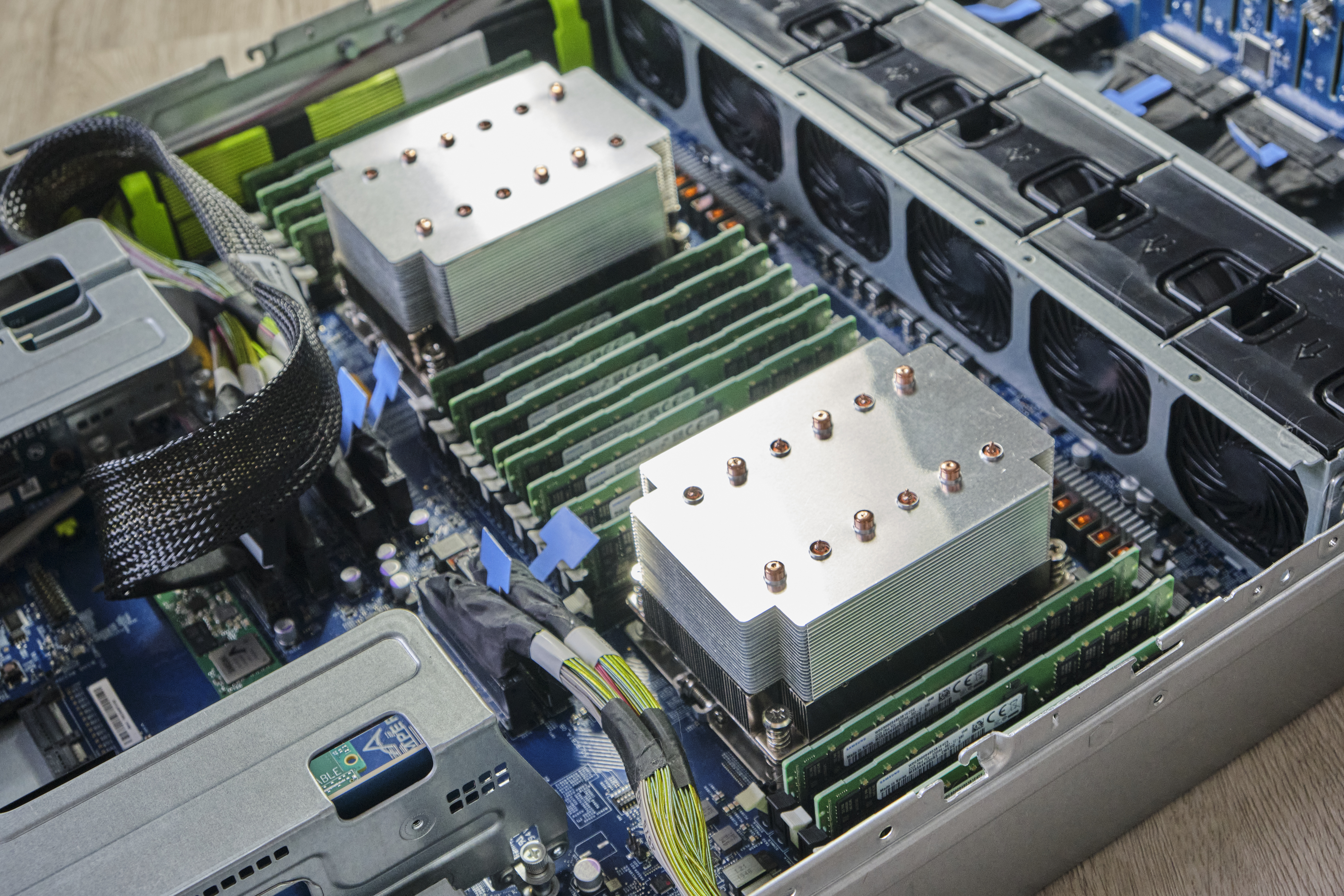
Although it’s a massive chip with a huge IHS, the Mount Jade server surprised me with its cooling solution as the included 250W type cooler only made contact with about 1/4th the surface area of the heat spreader.
Ampere here doesn’t have a recessed “lip” around the IHS for the mounting bracket to hold onto the chip like on AMD or Intel systems, so the actual IHS surface is actually recessed in relation to the bracket which means you cannot have a flat surface cooler design across the whole of the chip surface.

Instead, the included 250W design cooler uses a huge vapour chamber design with a “pedestal” to make contact with the chip. Ampere explains that they’ve experimented with different designs and found that a smaller area pedestal actually worked better for heat dissipation – siphoning heat off from the actual chip die which is notably smaller than the IHS and chip package.
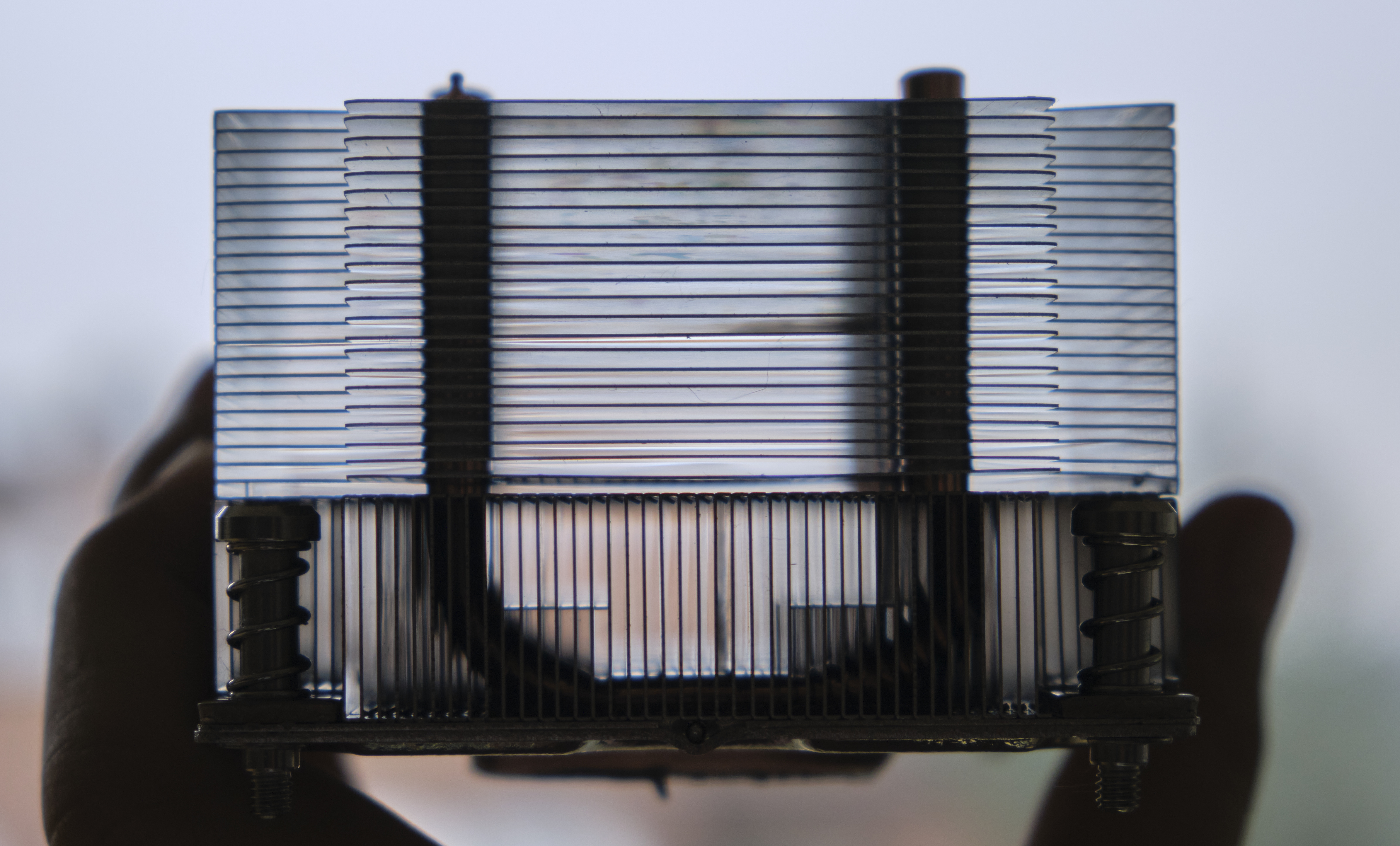
The cooler design is quite complex, with vertical fin stacks dissipating heat directly off the vapour chamber, with additional large horizontal fins dissipating heat from 6 U-shaped heat pipes that draw heat from the vapour chamber. It’s definitely a more complex and high-end design than what we’re used to in server coolers.
Although the Mount Jade server is definitely a very interesting piece of hardware, our focus today lies around the actual new Altra processors themselves, so let’s dive into the new Q80-33 80-core chip next.


148 Comments
View All Comments
mostlyfishy - Friday, December 18, 2020 - link
Interesting article thanks. One thing I missed, what process is this on? 7nm?It's also interesting that the M1 has demonstrated that with the right sizings, a very wide backend can give you significant single threaded performance. Not really that useful for a server processor where you're likely to be running many threads and want to trade for more cores though.
Josh128 - Friday, December 18, 2020 - link
Yes, 7nm and monolithic, which seems fairly incredible as this thing is huge. Dont have the die size numbers though. Wonder what the yield is on these...Calin - Friday, December 18, 2020 - link
Maybe there are quite a few more than 80 cores on this beast - in which case you can "eat" some die errors by deactivating cores/complexes/...Wilco1 - Friday, December 18, 2020 - link
Each Neoverse N1 core with 1MB L2 is just 1.4mm^2, so 80 of them add up to 112mm^2. The die size is estimated at about 350mm^2, so tiny compared to the total ~1100mm^2 in EPYC 7742.So performance/area is >3x that of EPYC. Now that is efficiency!
andrewaggb - Friday, December 18, 2020 - link
Timing of this article is awkward. We're comparing to the 18 month old 7742 vs the soon to be released Zen 3 Milan parts which based on the already launched Zen 3 desktop parts (and Milan leaks) will be 9-27% faster in the same power envelope.Cache is a big part of the die size for the AMD chip and the N1 has much less of it which makes the die size smaller. AMD's Desktop IGP parts with way less cache perform very similarly in many workloads to those with the extra cache and the same has been true for intel parts over the years. Some workloads don't benefit much at all from the extra cache and some do which makes choosing the benchmarks more important.
That's not to say the N1 isn't more efficient, but rather that it's hard to make a fair comparison, particularly around die size. They may have similar core counts but have made very different design decisions around cache.
Wilco1 - Friday, December 18, 2020 - link
I don't see how it matters, but Altra is about 9 months old and Neoverse N1 is a sibling of Cortex-A76 which has been available in phones for 2 years. As for Milan, I expect the gain on SPECrate to be about 10-15%. And Milan will be competing with the Altra Max which has 60% more cores which should give ~40% speedup.Yes the design decisions are quite different, and it is interesting that they end up with similar performance despite the disparity in L3 cache. I suspect that 8 memory channels is becoming a limit, and a future generation with DDR5 will enable more throughput (and even more cores).
Gondalf - Friday, December 18, 2020 - link
I am sorry but looking carefully the heatsink and the application of the thermal paste, we are facing a limit of the reticle thing on 7nm.We are in front of a 700/800 mm2 thing. On 7nm this means very few units sold and nearly zero market penetration. Same thing on 5nm given the higher core numbers.
In pratics we have nothing in our hands. Another failure in Server market
Andrei Frumusanu - Friday, December 18, 2020 - link
Ampere is doing Altra Max with 128 cores still on 7nm, so this one certainly isn't near hitting reticle limits.Wilco1 - Friday, December 18, 2020 - link
No it is not anywhere near the reticle limit. You can't estimate the die size from the heatsink, but you estimate it based on similar designs for which we do have numbers. Graviton 2 is a similar design at 30B transistors. This has another 16 cores which adds another 16X1.4 = 22.4mm^2. So around 350mm^2 in N7.milli - Monday, December 21, 2020 - link
This is just a ridiculous statement. 350mm^2 ... no way.Firstly, the die size of Graviton 2 is not known.
A realistic comparison would be AMD's Zen2 chiplet which has 3.9b transistors and is 72mm^2.
One would deduce from that, that Graviton 2 is > 550mm^2. Also your napkin calculation to add 22mm2 is flawed. Firstly, you don't know if a N1 core is actually taking 1.4mm^2 in this CPU. Secondly, you're forgetting to add 64 PCI-E lanes.
Let's say, 25mm2 for the CPU and 25mm2 for the lanes. That would bring the total to 600mm^2. Quite a bit bigger to your 350mm^2.