EUV Wafers Processed and TwinScan Machine Uptime: A Quick Look
by Dr. Ian Cutress on December 11, 2019 5:15 PM EST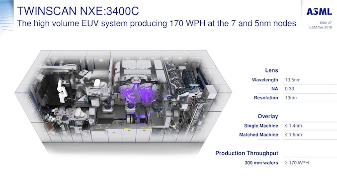
One of the interesting elements that came out of some of our discussions at the IEDM conference this year revolves around the present deployment of EUV. Currently only one company makes EUV tools, ASML, and the deployment of these to the various foundries that are on the leading edge has been a topic of some discussion here at the event, especially as we start talking about 7nm, 5nm, 3nm, and new generations of tools.
One of the interesting metrics that we’ve seen from ASML is the total number of 300mm wafers that have been enabled through EUV. Early adoption of EUV actually started all the way back in 2013, and it took until 2017 to push through over 1,000,000 wafers. In 2018 another 900,000 wafers were processed, and through 2019, with chips such as Huawei’s Kirin 990 5G, Qualcomm’s upcoming Snapdragon 700 series, and Samsung’s own EUV efforts, another 2.5 million wafers have been processed, showing an explosive CAGR of 95% since 2016.
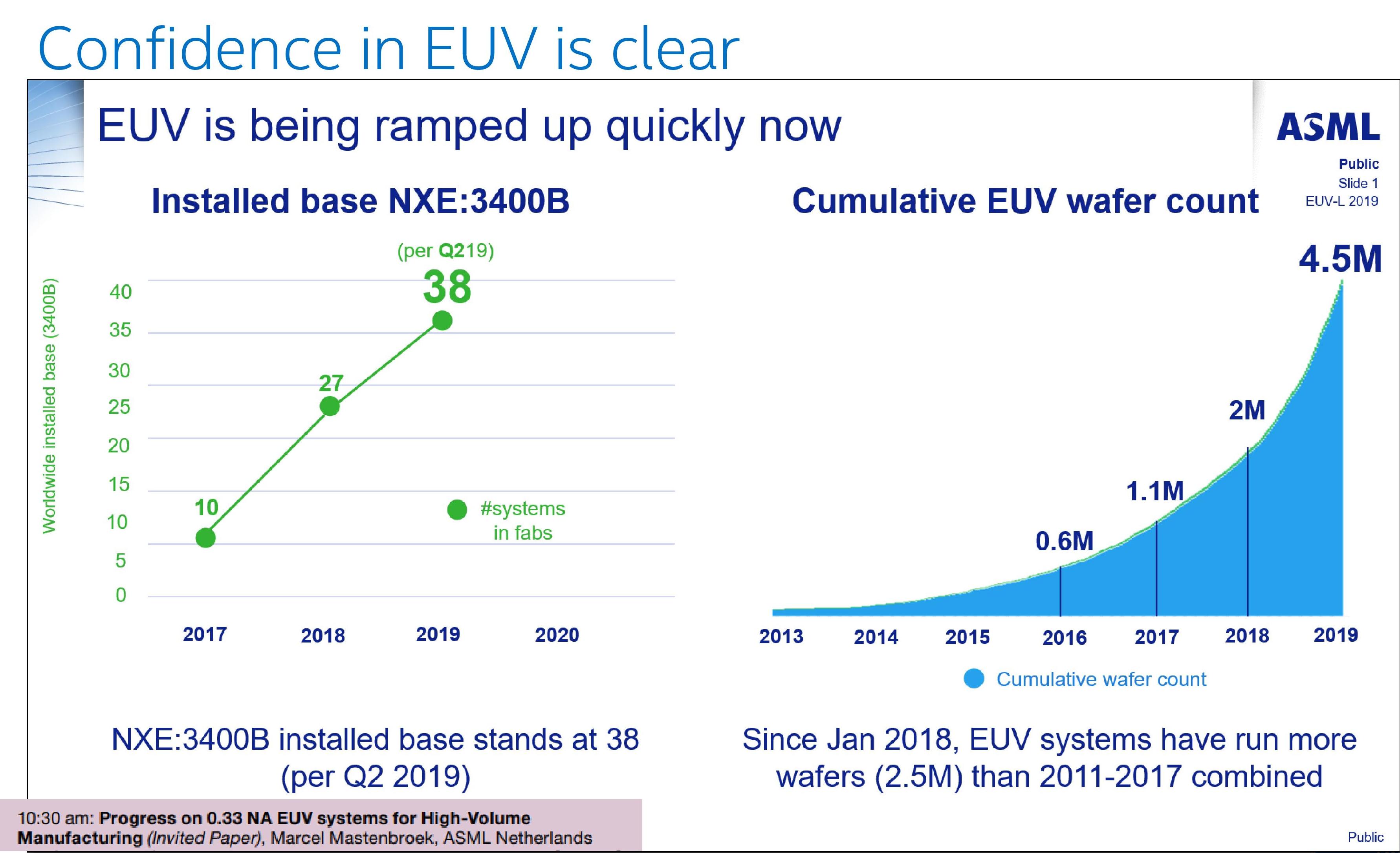
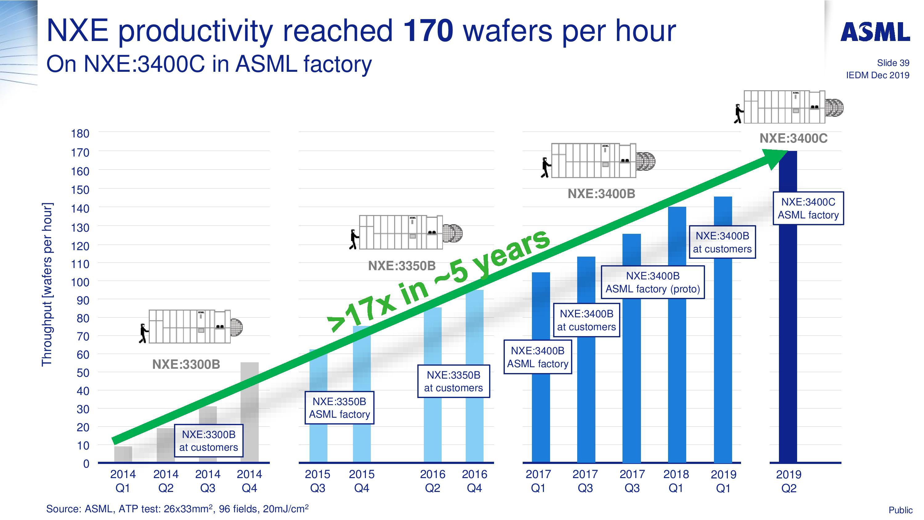
Along with that, ASML’s NXE:3400B Step and Scan machines have been at the heart of most of this EUV production. As the graph above shows, 38 machines were installed by Q2 2019, and through 2019 the B versions have been replaced with the NXE:3400C editions, which can process at peak 175 wafers per hour.
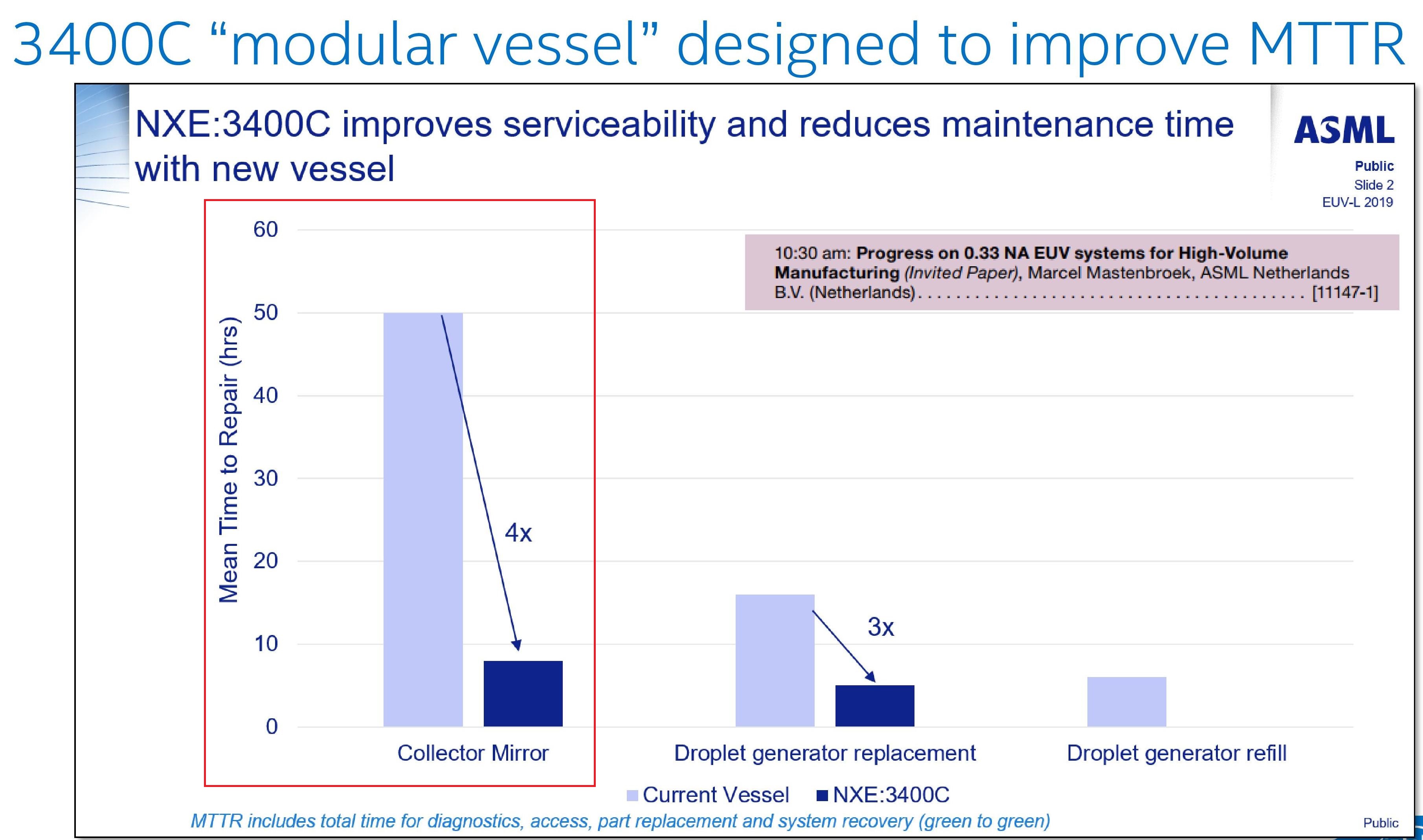
One of the advantages of the NXE:3400C models is the modularity in its design, meaning that a mirror defect should take only an 8-10 hour replacement, rather than take the machine out of action for a full 48 hours.
A note on EUV machine uptime is a key metric: ASML states that their average uptime (a 13-week moving average) is around 75%. This includes a series of ongoing updates to the machines, whcih take about 10% of that downtime: customers who want persistance on their machines without direct updates (or less frequent updates) end up with an average uptime of around 85%.
(Update: originally this article quoted uptimes from a different machine due to a miscommunication. The article has been updated to reflect ASML's latest numbers.)
ASML is keen to promote its improvement in wafer throughput of its NXE machines, from a little over 10 wafers per hour in 2014 to 170-175 in 2019.
Beyond the NXE lines of machines will be the EXE:5000 series. What makes these machines different is that they are built for the equivalent of TSMC’s 3nm / Intel’s 5nm processes by using ‘High-NA’ technology, technically moving from 0.33 NA optics to 0.55 NA optics, which will help improve manufacturing features at smaller and smaller resolutions. It will be interesting to see if the speed of the High-NA EXE machines will be similar or better to the NXE machines. Based on ASML’s presentation, High-NA machines should be coming into the market by 2023, by which time EUV use should be extensive at the leading edge.
Related Reading
- EUV Demand is Up: EUV Device Manufacturer ASML Beats Sales Estimates
- ASML to Ship 30 EUV Scanners in 2019: Faster EUV Tools Coming
- ASML Ships Twinscan NXT:2000i Scanner for 7nm and 5nm DUV
- Intel’s Manufacturing Roadmap from 2019 to 2029: Back Porting, 7nm, 5nm, 3nm, 2nm, and 1.4 nm
- Samsung Announces Exynos 990: 7nm EUV, M5, G77, LPDDR5 Flagship SoC alongside Exynos 5123 5G Modem
- TSMC: N7+ EUV Process Technology in High Volume, 6nm (N6) Coming Soon
- Samsung Announces the Exynos 9825 SoC: First 7nm EUV Silicon Chip
- Samsung’s Aggressive EUV Plans: 6nm Production in H2, 5nm & 4nm On Track


29 Comments
View All Comments
FullmetalTitan - Thursday, December 12, 2019 - link
Enough with your conspiracy theory. There is a 0% chance that Intel was secretly using EUV all along because, as market watchers can easily prove to you, 100% of the NXE3400B scanners were pre-purchased by Samsung and TSMC for 2 consecutive years (2017/2018).Yojimbo - Saturday, December 14, 2019 - link
I'm not defending anything. I am questioning why you think Intel would say they are not using EUV on a process node when they in fact are. What would ASML think about that? Obviously ASML knows whether they are or are not doing that. It just wouldn't look good. ASML is a long-term partner. And what's the reason, anyway? What does Intel get out of it? It just makes little sense to me, and you haven't made any argument that provides a reasonable motive for them to do so. As far as I can see, your whole argument is "It would make them look worse." Why would it look worse if they said they used EUV? Do you realize that all these companies participate in industry conferences where they share various data on matters that concern the whole industry. Some of those matters would be necessary developments from other companies in order to make EUV insertion more efficient. If Intel were hiding their true experience with EUV they would not be able to make these observations public, thus shooting themselves in the foot. Just because someone has the opportunity to commit a crime ("they could possibly have the machines") and the character to commit a crime ("Intel has deceptive marketing", doesn't mean it's been committed by them. Without a convincing motive for them to do something weird like hiding the use of EUV it's just nonsense.Fataliity - Wednesday, December 11, 2019 - link
Oh look, your the same guy defending Intel on the other article. and yes, they struggled for what? Like 5 years? 10nm completely failed. Only chip to come out was graphic disabled i3. 2 core i think. Now Ice Lake is 10nm+. Which if that chart is accurately representing Ice Lake (which I believe it may be), that means end of 2018 they finally sorted out their issues, which corresponds to them saying that their 10nm is ahead of schedule and doing well. It doesn't show yields but I'm sure that this was what they were referencing when they said ahead of schedule. The uptime.Yojimbo - Saturday, December 14, 2019 - link
You obviously have a hatred for Intel, and I think it's clouding your judgment. I have no particular love for Intel. I think the company has become a corporate boondoggle and is wasting a lot of money. But I also see people that seen to resent Intel just because they are big and successful, and those people say things that confirm their biases and wishes without fully considering the situations. As an example, in the other article, where people conveniently show no awareness of the differences between Intel's position and TSMC's that can make a process successful for TSMC which would be a failure for Intel.As for what you just said, if TSMC can get their 7 nm to work OK without EUV then why can't Intel get their 10 nm to work? They just needed more time. From what I've seen, insertion of EUV in a process is a big deal and it demands a major redesign. Sure it's possible Intel helped their 10 nm problems by using EUV, but why wouldn't they just say that? Anyway, I've had enough of this topic. You can be sure of whatever you want.
Ex EUV guy - Wednesday, December 11, 2019 - link
If they had not decreased funding for EUV in 2005, they could have had it a year or two earlier.edzieba - Thursday, December 12, 2019 - link
"It will be interesting to see if the speed of the High-NA EXE machines will be similar or better to the NXE machines."High-NA = hayai, na?
ksec - Thursday, December 12, 2019 - link
Wanted to point out TSMC 3nm is aiming at 2022. i.e High NA EUV are likely for 2nm if not 1.4nm.name99 - Friday, December 13, 2019 - link
3nm will mean whatever TSMC wants it to mean, ie whatever is ready to roll out in 2022.This MAY be smaller lithography (driven by high NA).
OR it may mean GAA transistors at 5nm lithography.
OR it may mean new materials
OR...
That's why TSMC is king: because they're testing multiple things simultaneously, but they only move the non-risky ones into production, AND they don't shoot their mouths off about what they'll be doing ten years from now, so they have no particular stake in what "defines" the 3nm node. 3nm will be exactly what I said -- all the stuff that's ready to roll in 2022, none of the stuff that isn't.
ballsystemlord - Friday, February 7, 2020 - link
Spelling error:"...whcih take about 10% of that downtime:..."
which is misspelled:
"...which take about 10% of that downtime:..."