EUV Wafers Processed and TwinScan Machine Uptime: A Quick Look
by Dr. Ian Cutress on December 11, 2019 5:15 PM EST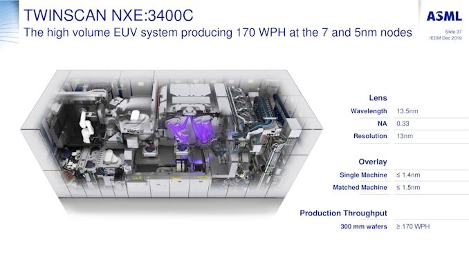
One of the interesting elements that came out of some of our discussions at the IEDM conference this year revolves around the present deployment of EUV. Currently only one company makes EUV tools, ASML, and the deployment of these to the various foundries that are on the leading edge has been a topic of some discussion here at the event, especially as we start talking about 7nm, 5nm, 3nm, and new generations of tools.
One of the interesting metrics that we’ve seen from ASML is the total number of 300mm wafers that have been enabled through EUV. Early adoption of EUV actually started all the way back in 2013, and it took until 2017 to push through over 1,000,000 wafers. In 2018 another 900,000 wafers were processed, and through 2019, with chips such as Huawei’s Kirin 990 5G, Qualcomm’s upcoming Snapdragon 700 series, and Samsung’s own EUV efforts, another 2.5 million wafers have been processed, showing an explosive CAGR of 95% since 2016.
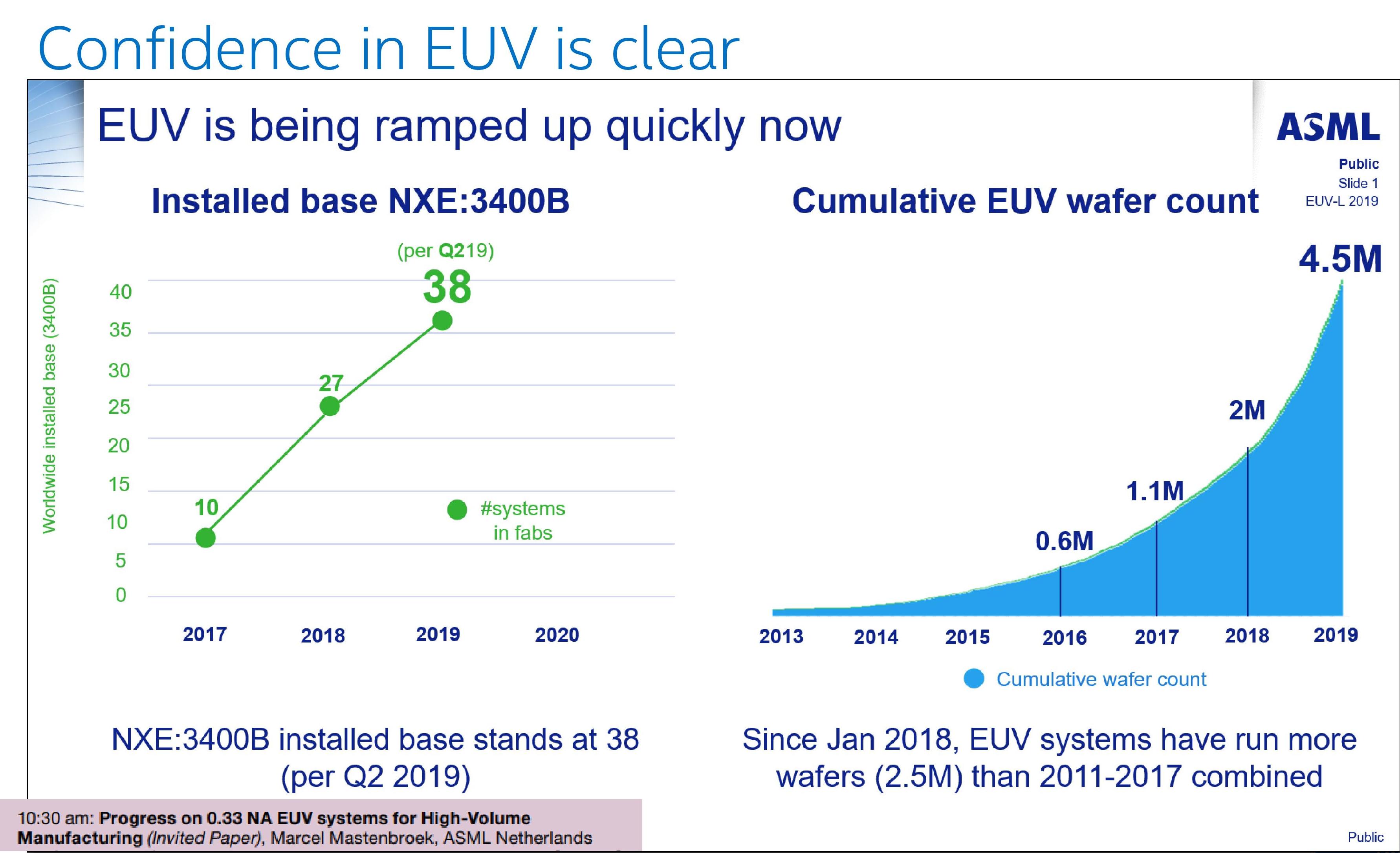
Along with that, ASML’s NXE:3400B Step and Scan machines have been at the heart of most of this EUV production. As the graph above shows, 38 machines were installed by Q2 2019, and through 2019 the B versions have been replaced with the NXE:3400C editions, which can process at peak 175 wafers per hour.
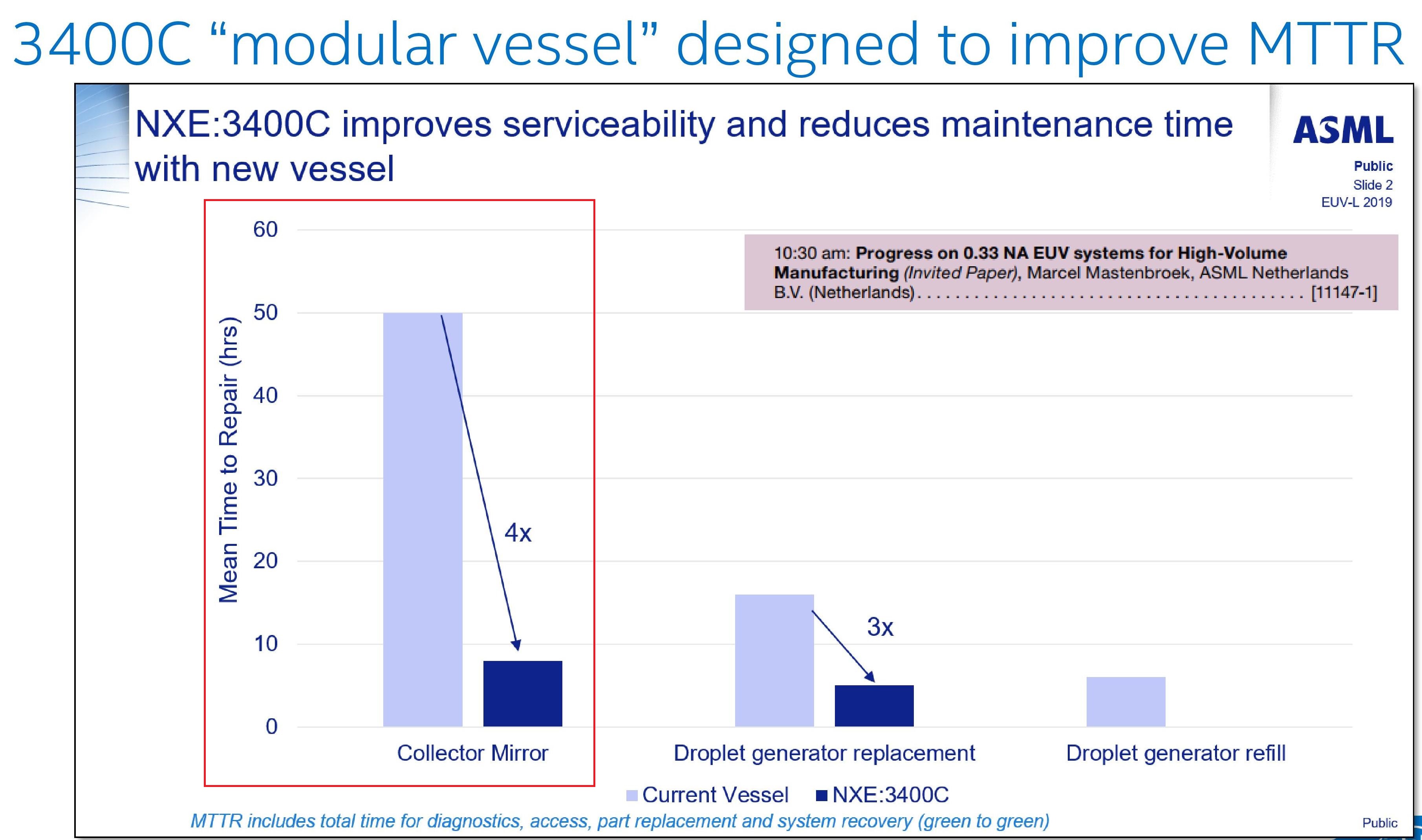
One of the advantages of the NXE:3400C models is the modularity in its design, meaning that a mirror defect should take only an 8-10 hour replacement, rather than take the machine out of action for a full 48 hours.
A note on EUV machine uptime is a key metric: ASML states that their average uptime (a 13-week moving average) is around 75%. This includes a series of ongoing updates to the machines, whcih take about 10% of that downtime: customers who want persistance on their machines without direct updates (or less frequent updates) end up with an average uptime of around 85%.
(Update: originally this article quoted uptimes from a different machine due to a miscommunication. The article has been updated to reflect ASML's latest numbers.)
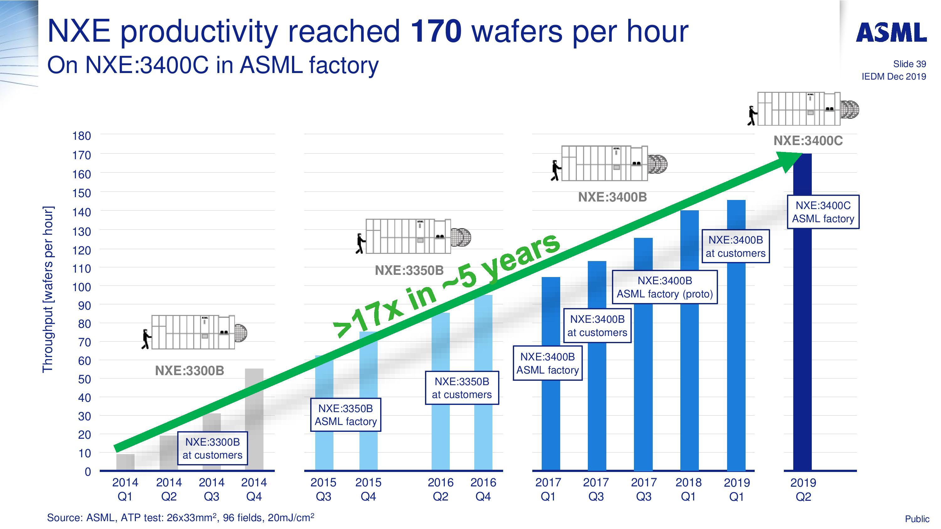
ASML is keen to promote its improvement in wafer throughput of its NXE machines, from a little over 10 wafers per hour in 2014 to 170-175 in 2019.
Beyond the NXE lines of machines will be the EXE:5000 series. What makes these machines different is that they are built for the equivalent of TSMC’s 3nm / Intel’s 5nm processes by using ‘High-NA’ technology, technically moving from 0.33 NA optics to 0.55 NA optics, which will help improve manufacturing features at smaller and smaller resolutions. It will be interesting to see if the speed of the High-NA EXE machines will be similar or better to the NXE machines. Based on ASML’s presentation, High-NA machines should be coming into the market by 2023, by which time EUV use should be extensive at the leading edge.
Related Reading
- EUV Demand is Up: EUV Device Manufacturer ASML Beats Sales Estimates
- ASML to Ship 30 EUV Scanners in 2019: Faster EUV Tools Coming
- ASML Ships Twinscan NXT:2000i Scanner for 7nm and 5nm DUV
- Intel’s Manufacturing Roadmap from 2019 to 2029: Back Porting, 7nm, 5nm, 3nm, 2nm, and 1.4 nm
- Samsung Announces Exynos 990: 7nm EUV, M5, G77, LPDDR5 Flagship SoC alongside Exynos 5123 5G Modem
- TSMC: N7+ EUV Process Technology in High Volume, 6nm (N6) Coming Soon
- Samsung Announces the Exynos 9825 SoC: First 7nm EUV Silicon Chip
- Samsung’s Aggressive EUV Plans: 6nm Production in H2, 5nm & 4nm On Track


29 Comments
View All Comments
Yojimbo - Wednesday, December 11, 2019 - link
No, Intel did not use EUV in their 10 nm, and that's one reason they had so much trouble with it. If EUV ad been available at their original 10 nm insertion the whole thing would have been easier.ksec - Thursday, December 12, 2019 - link
No EUV machines are going to Intel, and their 10nm isn't using EUV.ASML has limited capacity to make their TwinScan, and currently all of those are going to TSMC and Samsung. And if TSMC were to have 5nm in HVM by H1 2020, you can bet majority of those are going to TSMC.
The cumulative wafer are also deceptive and does not in anyway represent shipment. At 100mm Die size, 2.5M Wafer would have come out to nearly 625M unit.
Speedfriend - Friday, December 13, 2019 - link
Intel definitely has EUV machines, they are using them on 7nm. They funded the development of EUV together with TSMC and SamsungFataliity - Wednesday, December 11, 2019 - link
newsroom.intel [dot] com/news/2019-intel-investor-meeting/This meeting would've taken place right near the end of Intel's chart shown there. (Also just re-reading it, the graphics part is funny. They say 2x graphical performance of Ice Lake with ddr-4 4266mhz memory (versus 3733mhz on other tests) compared to old HD graphics at ddr3-1866mhz memory). and compared on a 5c 5thread versus a 2c 4t cpu. Very odd comparison ;) Everyone knows memory bandwidth affects graphics very heavily. and at resolution the cores would affect graphics too
www.theverge [dot] com/2018/10/22/18009784/intel-10nm-chips-canceled-report-comment
This would be week 43 2018. Which is right after their huge scheduled downtime and their first uptick in uptime hours close to a 24hour production shift.
techreport[dot]com/news/33947/intel-sees-excellent-q2-2018-results-amidst-news-of-10-nm-delays/
All of these reports, when comparing to this slide, correspond with waiting for EUV machines, and match with their reports about 10nm. Something in 10nm is using EUV that they couldn't do with DUV. and judging by the graph, I bet the big red scheduled downtime before production became 24hour shifts was infact installing a second EUV machine in the line somewhere.
All of the pieces match. Intel's 10nm+ is TSMC's 7nm+ in a sense, EUV layers and DUV layers. Intel's hold back is currently just machines that can produce EUV chips, hence laptop only. I wonder how many machines of EUV intel has, can you find out? Can calculate wafers/hour and match with their 10nm laptop sales. I bet they would match up very closely.
Yojimbo - Wednesday, December 11, 2019 - link
No. Intel is not using EUV, and timing wise, even if they had added EUV to their 10 nm lines it would have had to be after they already had problems with the original 10 nm that was based entirely on DUV.It's hard to know how many EUV machines Intel has, but they would rather be using them for their upcoming 7 nm node, and as someone else pointed out, it doesn't make sense for them to lie about not using EUV on the node.
Fataliity - Wednesday, December 11, 2019 - link
After all the lying and deceptive marketing towards AMD recently regarding benchmarks and comparisons, your really going to say it doesn't make sense for them to lie about using EUV in their 10nm+ vs their failed 10nm DUV? They are saving face. And also, 14nm++ is extending into 2020 for desktop and server chips. You could argue that once they have enough EUV machines, they will transition directly from 14nm++ to 7nm in those product segments and transition the 10nm+ lines directly to 7nm also. Why make it high volume if your going to basically leapfrop it?And regarding the latest slide Anandtech showed, with backport capability. 10nm++ to 7nm backport. If you use Ian's logic of each plus basically representing a different node (like 9nm, 8nm), the backporting becomes more logical. Because as they transition to ++ and EUV backward compatibility will be easy. Basically as long as the transitors and gates are at a set percentage throughout the design, they can just scale up design (120% transitor, 140% gate, etc) and make the design backward compatible easily instead of optimizing specifically for each node characteristic to extract maximum performance.
Look at the bigger picture..
Fataliity - Wednesday, December 11, 2019 - link
Because as they install the EUV machines, if they are capable of 7nm why wouldn't they be capable of 10nm++? That's why the new strategy exists. The new machines are capable of much more so just making the design bigger if they run into problems is much easier when they are using next-gen technology versus DUV.Yojimbo - Thursday, December 12, 2019 - link
Yes, I am going to say that. Because, regardless of what "lying and deceptive marketing towards AMD" you are talking about (why is Intel marketing their products towards AMD?), they would presumably have some reason of doing so. They do not have any reason to lie about using EUV. I don't see why you think a backport will be "easy" to implement if they both use EUV. For example, even if they were to both use EUV they would probably use it for a different number of layers. It just sounds like you are blowing smoke here. I don't think they can "just scale up the design". Laying out a chip is very complicated and the characteristics of the transistors change what the optimal layout is. They need to worry about hotspots. There are different parts of the entire chip assembly, i.e., the beol, feol, etc., that have different purposes. I have no idea what leaving open the option to backport entails, but I am sure you don't either.Fataliity - Thursday, December 12, 2019 - link
Their deceptive marketing towards comparing their products toward AMD's is due to their inefficiency and uncompetitive current lineup. Trying to change which benchmarks are used, co-developing AI-XPRT, and another one i forget, getting user benchmark to change the score weightings to lower AMD's score, recommending people benchmark with tools like matlab (Intel Compiler, cripples AMD to SSE but if you write a batch script to trick the program into thinking its Intel, it will run full speed on AVX.)Everything Intel does reflects on the company they have become. Why would they admit they failed 10nm and use EUV for 10nm+? It would make them look worse. Especially because their yields on 10nm are very low and they haven't been able to scale it to server and desktop yet, after 5-6 years.
There's alot of reasons to lie. And once they get more EUV machines and work out the kinks for 7nm, they will adjust the 10nm+ line last and just easily convert to 7nm. Simple as that.
And if their transistors placement and gates are a certain percentage different across the entire product (20% smaller, etc), it makes backporting much easier. They can just scale the design and have an engineer rework the circuits for the increased space. Same way Vega was made on 7nm with very little effort for the Radeon VII.
No more specific-characteristic of node optimizations, they are creating a system where everything is relative per node, so designs can be scaled by the relative difference. Yes it's a little more technical than that, but that's basically how it works. When you specifically optimize for specific parts of a node that are design rules that can only benefit the characteristics of that particular node, you have to re-design it for a different node. If you lower the rules and make common rules across nodes, backporting is much easier. You don't have edge-cases that have to be redesigned, everything is compatible. (It also makes it have less performance because of that, but the +'s are specific optimizations.)
Fataliity - Thursday, December 12, 2019 - link
I really don't understand what your defending. It's not a fanboy argument, it's the reality of the situation. We can disagree on whether or not EUV is used because they won't disclose it and the people working on it are NDA bound, but if you think about it instead of just dismissing it - it makes alot of sense given the situation they are in.