The Snapdragon 865 Performance Preview: Setting the Stage for Flagship Android 2020
by Andrei Frumusanu on December 16, 2019 7:30 AM EST- Posted in
- Mobile
- Qualcomm
- Smartphones
- 5G
- Cortex A77
- Snapdragon 865
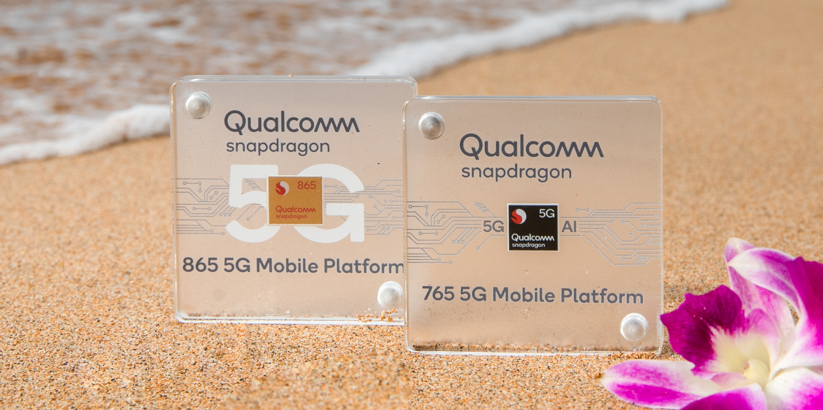
Earlier this month we had the pleasure to attend Qualcomm’s Maui launch event of the new Snapdragon 865 and 765 mobile platforms. The new chipsets promise to bring a lot of new upgrades in terms of performance and features, and undoubtedly will be the silicon upon which the vast majority of 2020 flagship devices will base their designs on. We’ve covered the new improvements and changes of the new chipset in our dedicated launch article, so be sure to read that piece if you’re not yet familiar with the Snapdragon 865.
As has seemingly become a tradition with Qualcomm, following the launch event we’ve been given the opportunity to have some hands-on time with the company’s reference devices, and had the chance to run the phones through our benchmark suite. The QRD865 is a reference phone made by Qualcomm and integrates the new flagship chip. The device offers insight into what we should be expecting from commercial devices in 2020, and today’s piece particularly focuses on the performance improvements of the new generation.
- Qualcomm Announces Snapdragon 865 and 765(G): 5G For All in 2020, All The Details
- Qualcomm Windows on Snapdragon: New 7c & 8c SoCs for sub-$800 Laptops
- Quick Bytes: Qualcomm’s Dynamic Spectrum Sharing Demo with 5G and 4G
- Quick Bytes: Qualcomm’s Prediction of 1.4 Billion 5G Smartphones by 2022
- Qualcomm Snapdragon Tech Summit Live Blog: Day One
- Qualcomm Snapdragon Tech Summit Live Blog Day Two: All About Mobile
- Qualcomm Snapdragon Tech Summit Day 3 Live Blog: ACPC and XR
A quick recap of the Snapdragon 865 if you haven’t read the more thorough examination of the changes:
| Qualcomm Snapdragon Flagship SoCs 2019-2020 | |||
| SoC |
Snapdragon 865 |
Snapdragon 855 | |
| CPU | 1x Cortex A77 @ 2.84GHz 1x512KB pL2 3x Cortex A77 @ 2.42GHz 3x256KB pL2 4x Cortex A55 @ 1.80GHz 4x128KB pL2 4MB sL3 @ ?MHz |
1x Kryo 485 Gold (A76 derivative) @ 2.84GHz 1x512KB pL2 3x Kryo 485 Gold (A76 derivative) @ 2.42GHz 3x256KB pL2 4x Kryo 485 Silver (A55 derivative) @ 1.80GHz 4x128KB pL2 2MB sL3 @ 1612MHz |
|
| GPU | Adreno 650 @ 587 MHz +25% perf +50% ALUs +50% pixel/clock +0% texels/clock |
Adreno 640 @ 585 MHz |
|
| DSP / NPU | Hexagon 698 15 TOPS AI (Total CPU+GPU+HVX+Tensor) |
Hexagon 690 7 TOPS AI (Total CPU+GPU+HVX+Tensor) |
|
| Memory Controller |
4x 16-bit CH @ 2133MHz LPDDR4X / 33.4GB/s or @ 2750MHz LPDDR5 / 44.0GB/s 3MB system level cache |
4x 16-bit CH @ 1866MHz LPDDR4X 29.9GB/s 3MB system level cache |
|
| ISP/Camera | Dual 14-bit Spectra 480 ISP 1x 200MP 64MP ZSL or 2x 25MP ZSL 4K video & 64MP burst capture |
Dual 14-bit Spectra 380 ISP 1x 192MP 1x 48MP ZSL or 2x 22MP ZSL |
|
| Encode/ Decode |
8K30 / 4K120 10-bit H.265 Dolby Vision, HDR10+, HDR10, HLG 720p960 infinite recording |
4K60 10-bit H.265 HDR10, HDR10+, HLG 720p480 |
|
| Integrated Modem | none (Paired with external X55 only) (LTE Category 24/22) DL = 2500 Mbps 7x20MHz CA, 1024-QAM UL = 316 Mbps 3x20MHz CA, 256-QAM (5G NR Sub-6 + mmWave) DL = 7000 Mbps UL = 3000 Mbps |
Snapdragon X24 LTE (Category 20) DL = 2000Mbps 7x20MHz CA, 256-QAM, 4x4 UL = 316Mbps 3x20MHz CA, 256-QAM |
|
| Mfc. Process | TSMC 7nm (N7P) |
TSMC 7nm (N7) |
|
The Snapdragon 865 is a successor to the Snapdragon 855 last year, and thus represents Qualcomm’s latest flagship chipset offering the newest IP and technologies. On the CPU side, Qualcomm has integrated Arm’s newest Cortex-A77 CPU cores, replacing the A76-based IP from last year. This year Qualcomm has decided against requesting any microarchitectural changes to the IP, so unlike the semi-custom Kryo 485 / A76-based CPUs which had some differing aspects to the design, the new A77 in the Snapdragon 865 represents the default IP configuration that Arm offers.
Clock frequencies and core cache configurations haven’t changed this year – there’s still a single “Prime” A77 CPU core with 512KB cache running at a higher 2.84GHz and three “Performance” or “Gold” cores with reduced 256KB caches at a lower 2.42GHz. The four little cores remain A55s, and also the same cache configuration as well as the 1.8GHz clock. The L3 cache of the CPU cluster has been doubled from 2 to 4MB. In general, Qualcomm’s advertised 25% performance uplift on the CPU side solely comes from the IPC increases of the new A77 cores.
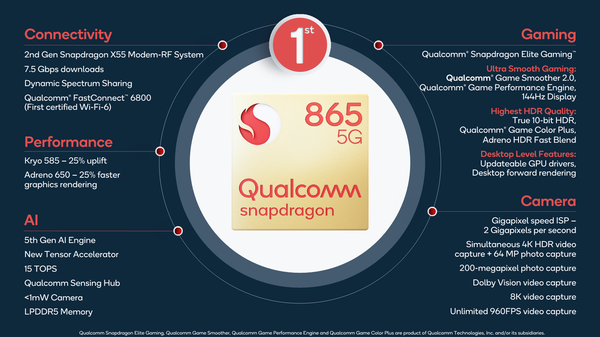
The GPU this year features an updates Adreno 650 design which increases ALU and pixel rendering units by 50%. The end-result in terms of performance is a promised 25% upgrade – it’s likely that the company is running the new block at a lower frequency than what we’ve seen on the Snapdragon 855, although we won’t be able to confirm this until we have access to commercial devices early next year.
A big performance upgrade on the new chip is the quadrupling of the processing power of the new Tensor cores in the Hexagon 698. Qualcomm advertises 15 TOPS throughput for all computing blocks on the SoC and we estimate that the new Tensor cores roughly represent 10 TOPS out of that figure.
In general, the Snapdragon 865 promises to be a very versatile chip and comes with a lot of new improvements – particularly 5G connectivity and new camera capabilities are promised to be the key features of the new SoC. Today’s focus lies solely on the performance of the chip, so let’s move on to our first test results and analysis.
New Memory Controllers & LPDDR5: A Big Improvement
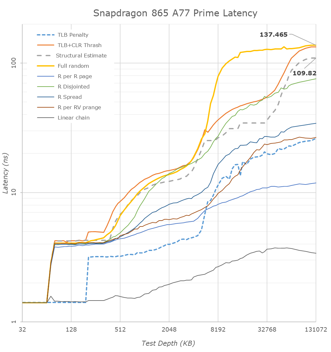
One of the larger changes in the SoC this generation was the integration of a new hybrid LPDDR5 and LPDDR4X memory controller. On the QRD865 device we’ve tested the chip was naturally equipped with the new LP5 standard. Qualcomm was actually downplaying the importance of LP5 itself: the new standard does bring higher memory speeds providing better bandwidth, however latency should be the same, and power efficiency benefits, while there, shouldn’t be overplayed. Nevertheless, Qualcomm did claim they focused more on improving their memory controllers, and this year we’re finally seeing the new chip address some of the weaknesses exhibited by the past two generations; memory latency.
We had criticised Qualcomm’s Snapdragon 845 and 855 for having quite bad memory latency – ever since the company had introduced their system level cache architecture to the designs, this aspect of the memory subsystem had seen some rather mediocre characteristics. There’s been a lot of arguments in regards to how much this actually affected performance, with Qualcomm themselves naturally downplaying the differences. Arm generally notes a 1% performance difference for each 5ns of latency to DRAM, if the differences are big, it can sum up to a noticeable difference.
( )
Looking at the new Snapdragon 865, the first thing that pops up when comparing the two latency charts is the doubled L3 cache of the new chip. It’s to be noted that it does look that there’s still some sort of logical partitioning going on and 512KB of the cache may be dedicated to the little cores, as random-access latencies start going up at 1.5MB for the S855 and 3.5MB for the S865.
Further down in the deeper memory regions, we’re seeing some very big changes in latency. Qualcomm has been able to shave off around 35ns in the full random-access test, and we’re estimating that the structural latency of the chip now falls in at ~109ns – a 20ns improvements over its predecessor. While it’s a very good improvements in itself, it’s still a slightly behind the designs of HiSilicon, Apple and Samsung. So, while Qualcomm still is the last of the bunch in regards to its memory subsystem, it’s no longer trailing behind by such a large margin. Keep in mind the results of the Kirin 990 here as we go into more detailed analysis of memory-intensive workloads in SPEC on the next page.
Furthermore, what’s very interesting about Qualcomm’s results in the DRAM region is the behaviour of the TLB+CLR Trash test. This test is always hitting the same cache-line within a page across different, forcing a cache line replacement. The oddity here is that the Snapdragon 865 here behaves very differently to the 855, with the results showcasing a separate “step” in the results between 4MB and ~32MB. This result is more of an artefact of the test only hitting a single cache line per page rather than the chip actually having some sort of 32MB hidden cache. My theory is that Qualcomm has done some sort of optimisation to the cache-line replacement policy at the memory controller level, and instead the test hitting DRAM, it’s actually residing at on the SLC cache. It’s a very interesting result and so far, it’s the first and only chipset to exhibit such behaviour. If it’s indeed the SLC, the latency would fall in at around 25-35ns, with the non-uniform latency likely being a result of the four cache slices dedicated to the four memory controllers.
Overall, it looks like Qualcomm has made rather big changes to the memory subsystem this year, and we’re looking forward to see the impact on performance.


178 Comments
View All Comments
rpg1966 - Monday, December 16, 2019 - link
How is Apple so far ahead in some/many respects, given that Arm is dedicated to designing these microarchitectures?eastcoast_pete - Monday, December 16, 2019 - link
In addition to spending $$$ on R&D, Apple can optimize (tailor, really) its SoCs 100% to its OS and vice versa. Also, not sure if anybody has figures just how much the (internal) costs of Apple's SoCs are compared to what Samsung, Xiaomi etc. pay QC for their flagship SoCs. Would be interesting to know how much this boils down to costs.jospoortvliet - Monday, December 16, 2019 - link
I think cody I'd the big factor. Qualcomm and arm keep chips small for cost reasons. Apple throws transistors at the problem and cares little...s.yu - Monday, December 16, 2019 - link
I like the approach of throwing transistors :)generalako - Monday, December 16, 2019 - link
Can we stop with these excuses? What cost reasons? Whose stopping them from making two architectures then, letting OEMs decide which to use -- if Apple does it, why not them? Samsung aiming at large cores with their failed M4 clearly points towards a desire/intention to have larger cores that are more performant. Let's not make the assumption that there's no need here--there clearly is.Furthermore, where is the excuse in ARM still being on the A55 for the third straight year? Or Qualcomm being on their GPU architecture for 3 straight years, with so incremental GPU improvements the past two years that they not only let Apple both match and vastly surpass them, but are even getting matched by Mali?
There's simply no excuse for the laziness going on. ARM's architecture is actually impressive, with still big year-on-year IPC gains (whereas Apple has actually stagnated here the past two years). But abandoning any work on efficiency cores is inexcusable. As is the fact that none of the OEMs has done anything to deal with this problem.
Retycint - Monday, December 16, 2019 - link
Probably because ARM designs for general use - mobiles, tablets, TVs, cars etc, whereas Apple designs specifically for their devices. So naturally Apple is able to devote more resources and time to optimize for their platform, and also design cores/chips specific to their use (phone or tablet).But then again I'm an outsider, so the reality could be entirely different
generalako - Monday, December 16, 2019 - link
TIL using the same A55 architecture is "for general use" /sIf ARM had actually done their job and released efficiency cores more often, like Apple does every year, we'd have far more performant and efficient smartphones today across the spectrum. Flagship phones would benefit in idle use (including standby), and also in assigning far more resource-mild works to these cores than they do today.
But mid-range and low-end phones would benefit a huge amount here, with efficiency cores performing close to performance cores (often 1-2 older gen clocked substantially lower). That would also be cheaper, as it would make cluster of 2 performance cores not as necessary--fitting right in with your logic of making cheap designs for general use.
quadrivial - Monday, December 16, 2019 - link
There's a few reasons.Apple seems to have started before arm did. They launched their design just 2 years or so after the announcement of a64 while arm needed the usual 4-5 years for a new design. I don't believe apples designers are that much better than normal (I think they handed them the ISA and threatened to buy out MIPS if they didn't). Arm has never recovered that lead time.
That said, PA Semi had a bunch of great designers who has already done a lot of work with low power designs (mostly POWER designs if I recall correctly).
Another factor is a32 support. It's a much more complex design and doesn't do performance, power consumption, or die area any favors. Apple has ecosystem control, so they just dropped the complex parts and just did a64. This also drastically reduces time to design any particular part of the core and less time to verify everything meaning more time optimizing vs teams trying to do both at once.
Finally, Apple has a vested interest in getting faster as fast as possible. Arm and the mobile market want gradual performance updates to encourage upgrades. Even if they could design an iPhone killer today, I don't think they would. There's already enough trouble with people believing their phones are fast enough as is.
Apple isn't designing these chips for phones though. They make them for their pro tablets. The performance push is even more important for laptops though. The current chip is close to x86 in mobile performance. Their upcoming 5nm designs should be right at x86 performance for consumer applications while using a fraction of the power. They're already including a harvested mobile chip in every laptop for their T2. Getting rid of Intel on their MacBook air would do two things. It would improve profits per unit by a hundred dollars or so (that's almost 10% of low end models). It also threatens Intel to get them better deals on higher end models.
We may see arm move in a similar direction, but they can't get away with mandating their users and developers change architectures. Their early attempts with things like the surface or server chips (a57 was mostly for servers with a72 being the more mobile-focused design) fell flat. As a result, they seem to be taking a conservative approach that eliminates risk to their core market.
The success or failure of the 8cx will probably be extremely impactful on future arm designs. If it achieves success, then focusing on shipping powerful, 64-bit only chip designs seems much more likely. I like my Pixelbook, but I'd be willing to try an 8cx if the price and features were right (that includes support for Linux containers).
Raqia - Monday, December 16, 2019 - link
Nice post! You're right, it really does seem like Apple's own implementations defined the ARM v8.x spec given how soon after ARM's release their chips dropped. ARM is also crimped by the need to address server markets so their chips have a more complex cache and uncore hierarchies than Apple's and generally smaller caches with lower single threaded performance. Their customers' area budgets are also more limited compared to Apple who doesn't generally integrate a modem into their SoC designs.aliasfox - Monday, December 16, 2019 - link
I would also add that Qualcomm only makes a dozen or so dollars per chip, whereas Apple makes hundreds of dollars per newest generation iPhone and iPad Pro. Qualcomm's business model just puts them at a disadvantage in this case - they have to make a chip that's not only competitive in performance, but at a low enough cost that a) they can make money selling it, and b) handset vendors can make money using it. Apple doesn't really have to worry about that because for all intents and purposes, their chip division is a part of their mobile division.I wonder if it's in the cards for Apple to ever include both an Intel processor as well as a full fledged mobile chip in the future, working in the same way as integrated/discrete graphics - the system would primarily run on the A13x, with the Intel chip firing up for Intel-binary apps as needed.