Intel’s Xe for HPC: Ponte Vecchio with Chiplets, EMIB, and Foveros on 7nm, Coming 2021
by Dr. Ian Cutress on November 17, 2019 7:00 PM EST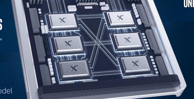
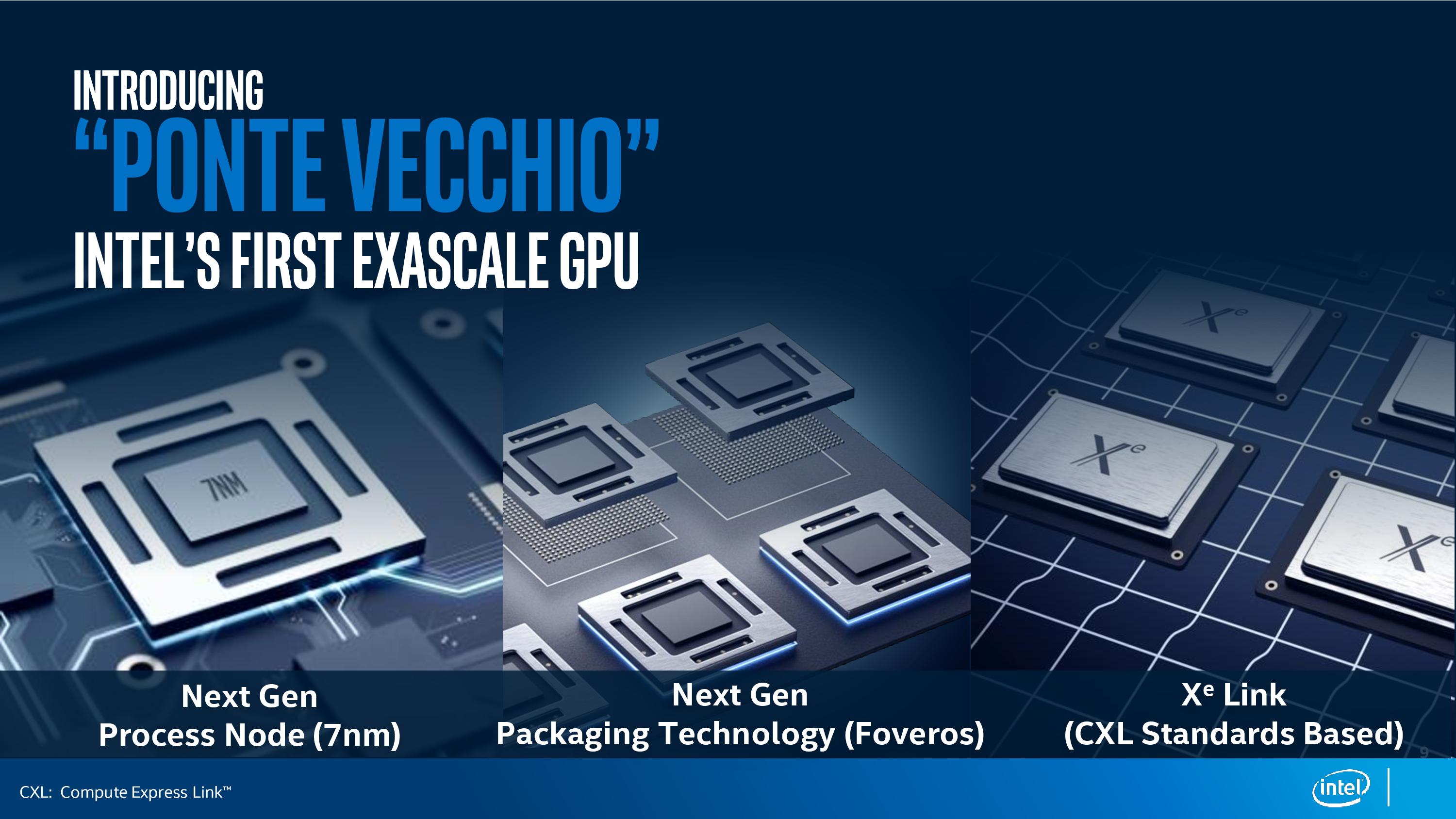
Today is Intel’s pre-SC19 HPC Devcon event, and with Raja Koduri on stage, the company has given a small glimpse into its high-performance compute accelerator strategy for 2021. Intel disclosed that its new hardware has the codename ‘Ponte Vecchio’ and will be built on a 7nm process, as well as some other small interesting bits.
Ever since Intel hired Raja Koduri from AMD’s Graphics division, the ambition in which Intel has been assembling its discrete GPU push has made for a strong injection of competition into this industry. Today a modern graphics architecture needs to be many things to many people: low powered for small chips, high performance for gaming and VR, perform sizable compute for HPC, and detail with different types of convolution and matrix math as AI becomes more important. Intel has already disclosed that its future products will bear its new ‘Xe’ architecture (that’s a superscript e), and that they plan to cover the spectrum all the way from integrated graphics to high performance computing, but that’s about all we have been told.

As part of the keynote speech today, Koduri has explained that Intel will have a single ‘Xe’ architecture but multiple sub-architectures / microarchitectures (or however you want to characterize it in a GPU) in order to address different parts of the market. The ultra-mobile parts of the product stack might focus on small die size and high efficiency libraries, whereas a compute product might have high double-precision performance and run high-performance libraries. Some variants might have the equivalent of tensor accelerators for AI, or some variants might have bigger cache variants to manage specific customer needs. Rather than a ‘one size fits all’ approach, it appears that Intel are going to stretch Xe as wide as they need to in order to accommodate as many customers as possible.

For high-performance computing, the presentation highlighted three key areas that the Xe architecture will be targeting. First is a flexible data-parallel vector matrix engine, which plays into the hands of AI acceleration and AI training in a big way. The second is high double precision (FP64) throughput, which has somewhat been disappearing of late due to reduced precision AI workloads, but is still a strong requirement in traditional HPC workloads like, weather, oil and gas, and astronomy. (We should point out that the diagram shows a 15x7 block of units, and Intel’s Gen architecture uses 7 threads per execution unit.) The third tine in this trident is that Intel’s HPC efforts will have a high cache and memory bandwidth, which the slides suggest will be directly coupled to individual compute chiplets ensuring a fast interconnect.
So in this case, enter Ponte Vecchio, named after the bridge that crosses the river Arno in Florence, Italy. This will be Intel’s first ‘exascale class’ graphics solution, and is clearly using both chiplet technology (based on 7nm) and Foveros/die stacking packaging methods. We further confirmed after our call, based on discussions we had with Intel earlier in the year, that Ponte Vecchio will also use Intel’s Embedded Multi-Die Interconnect Bridge (EMIB) technology, joining chiplets together. Pulling all the chips into a single package is fine, meanwhile GPU-to-GPU communication will occur through a Compute eXpress Link (CXL) interface, layered on top of PCIe 5.0.
So while this is an important development in the disclosure of Intel’s graphics strategy, specifically speaking to the HPC crowd, it still leaves a lot of questions to be answered: what exactly is Xe, how is compute handled differently from shaders, how has Intel solved the chiplet paradigm in GPUs (latency and bandwidth needs), how many chiplets per GPU, power consumption targets, what is stacked with Foveros, how is the memory connected, what type of memory, what are the performance targets, how many chiplets, what size of the chiplets, what exactly is 7nm, and so forth. What we do know at this point is that Intel is using a vector matrix engine, offers high FP64 performance, high memory bandwidth, and that for Intel, this is their ‘first exascale GPU’. In short, we're still in the early days of the Xe story, at least from a public perspective.
It’s worth noting that earlier this year, we were invited to discuss the future of Intel packaging with Ramune Nagisetty, who stated that technologies such as chiplets, Foveros (die stacking), and Intel’s Embedded Multi-Die Interconnect Bridge (EMIB) are all going to play critical roles in the future of Intel’s products, and specifically for the use the upcoming graphics portfolio. Part of that discussion was officially off the record, until today, such as the Ponte Vecchio code name. Ponte Vecchio (PV for short) is just one part of Intel’s Xe plans, as we have already been promised GPUs on 10nm.
Ponte Vecchio will be the showcase accelerator in the Aurora supercomputer, to be installed at Argonne National Laboratory in 2021. Intel has announced that this will feature two Sapphire Rapids CPUs (the one after Ice Lake), along with six Ponte Vecchio GPUs, in a single node. More details on this in our Aurora coverage.
Related Reading
- Intel's Interconnected Future: Combining Chiplets, EMIB, and Foveros
- Intel to Support Hardware Ray Tracing Acceleration on Data Center Xe GPUs
- Intel’s Xeon & Xe Compute Accelerators to Power Aurora Exascale Supercomputer
- Intel Details Manufacturing through 2023: 7nm, 7+, 7++, with Next Gen Packaging


16 Comments
View All Comments
Phynaz - Monday, November 18, 2019 - link
Still better than what AMD has in the HPC space.del42sa - Monday, November 18, 2019 - link
"Ponte Vecchio (PV for short) is just one part of Intel’s Xe plans, as we have already been promised GPUs on 10nm."yes, until now they were talking about 10nm. Now they skipped to 7nm.
Spunjji - Monday, November 18, 2019 - link
No solid information about the architecture, not even indications of how they think it will look... but it'll definitely be great!Sure, Intel. Sure.
JayNor - Saturday, December 7, 2019 - link
"IC: Is Xe anything like Gen at a fundamental level?RK: At the heart of Xe, you will find many Gen features.
...
So we preserved lots of the good elements of Gen, but we had to get an order of magnitude increase in performance. "
https://www.anandtech.com/show/15130/anandtech-exc...
Kevin G - Monday, November 18, 2019 - link
So far things look impressive on paper for the compute side of things. Intel is throwing a lot of silicon at performance and they seem to aiming for the performance crown. Too early to say anything about power consumption or efficiency.CXL based on PCIe 4.0 is going to be a good step forward for internal interconnect. Ian correctly pointed out that the diagrams does not match what they said in terms of topology. At a high level, it looks like each chiplet has an external package link and then an unknown number of internal links. That'd be the simple way to scale things for a true mesh topology between packages. More information is clearly needed here.
What is disappointed is the lack of detail on the node-to-node fabric. Omnipath is dead and could have been a late change in this design. Even without Omnipath, I find it surprising that they aren't leveraging their silicon photonics technology to move that aspect of communication in package as well. That'd be a straight forward way to enable 400 Gbit at scale for this system.
Santoval - Monday, November 18, 2019 - link
CXL runs on top of PCIe 5.0(+), not PCIe 4.0.