Hot Chips 31 Analysis: In-Memory Processing by UPMEM
by Dr. Ian Cutress on August 19, 2019 3:15 PM ESTInside the PIM-DRAM and DPU
So as mentioned, each data processing unit (DPU) is put in control of 64 MB of DRAM, leading to 128 DPUs in an 8 GB module. These are built into the DRAM at the same time as manufacturing, but the logic is not as physically dense as regular ASIC logic, making it a high-yielding solution. Ultimately a DRAM die is still mostly DRAM, and the UPMEM states that the DPU size is negligible by comparison. In order to do this, UPMEM created an ASIC-like framework of logic cells, SRAM IPs, and implementation flow. Ultimately the goal was to add these DPUs to an otherwise unmodified DRAM design, and the company states they have succeeded.
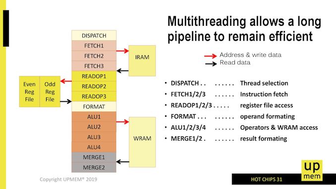
The DPU is a 14-stage interleaved pipeline processor, that uses 24 hardware threads to achieve better scaling (apparently only 11 are needed for 100% utilization). On multithreaded code, this creates a 1 instruction/cycle throughput, and the 1 GB/s latency per DPU to its local memory helps hide the threading. There is no operand bypass, and no stall signals.
Each DPU has 88 KB of SRAMs inside, split into 64 KB of WRAM (a data cache equivalent) and 24 KB of IRAM (instruction cache equivalent), with DMA instructions to move data between the DRAM and the WRAM/IRAM. These DMA engine is autonomous, which UPMEM states has little-no-effect on pipeline for performance. There is no actual ‘cache’ here, with the company stating that there are too many threads for actual caches, so instead they rely on the efficient DRAM engine and a tightly coupled bank of SRAM to do that job.
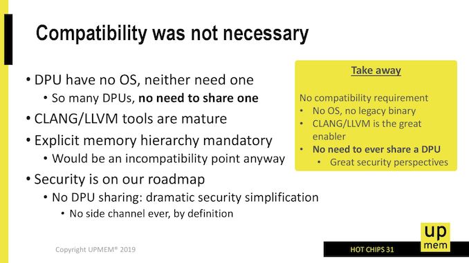
The 14-stage pipeline us a basic in-order threaded CPU with dispatch/fetch/read/format/ALU/merge stages with access to the local SRAMs. The DPU has a 64-bit wide access port to its 64 MB array of main DRAM for loads and stores through an immediate addressing mode, and ultimately control of the DPU is still through the main CPU. No DPU can talk to each other, and the DPUs can only work on their 64 MB of main memory, allowing security separation between the hardware.
The main server CPU has full control over the DPU units through the APIs provided by UPMEM, such that the DPUs can be done on an allocate/free bases or managed through group execution or one-by-one. The DPU doesn’t actually run an OS according to UPMEM, and is controlled just through the device driver.
UPMEM states that Clang and LLVM tools are mature to manage DPU use through the compiler and provided APIs. Technically the DPUs have orchestration overhead as a result, and part of this is down to using DDR4 rather than a proprietary interface. UPMEM states that this orchestration management, such as bus width mismatches, address interleaving, the lack of cache coherent and the lack of hardware arbitration, is negligible compared to the work the DPU actually does. The APIs for managing this are available for x86, POWER 9, and ARM64.
Internally the DPU uses an optimized 32-bit ISA with triadic instructions, with non-destructive operand compute. As mentioned, the optimized ISA contains a range of typical instructions that can easily be farmed out to in-memory compute, such as SHIFT+ADD/SHIFT+SUB, basic logic (NAND, NOR, ORN, ANDN, NXOR), shift and rotate instructions, and even compute that requires intermediate values. The DPU supports bi-endianess, and is host OS agnostic.
The Goal
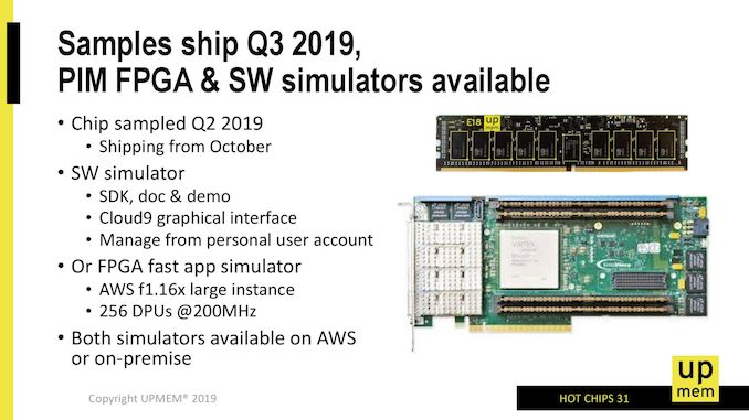
UPMEM is presenting its technology at Hot Chips as an attempt to attract potential customers, and is looking at mass production of its 8 GB memory modules in Q1, although early customers are already being sampled. The company is set to launch a sales office in the Bay Area during the second half of 2019.
The company is putting up impressive numbers for specific workloads, and to be honest, the question of in-memory compute is not really a question of if, but when. Even on the consumer side, there are some good examples where in-memory compute could help. I enjoyed going through UPMEM’s slide decks and looking at what they have to offer. It will be interesting to see other competing solutions come to the market, and how they approach the problem.
I will finish this article on one important note, however. Going up to 20W per 8 GB memory module is not a long-term solution. One of the disadvantages of moving compute away from the CPU is that you have to spend that compute power elsewhere, and a DRAM module isn’t usually the most ideal solution for that based on historic design (especially if doing the calculation is half as efficient). If a CPU socket can hold 150W, and a memory socket can do 20W, then you want most of the power consumed on the compute in the socket. In-memory compute is a good problem to solve, but ultimately it needs to be combined with on-CPU DRAM.


38 Comments
View All Comments
abufrejoval - Tuesday, August 20, 2019 - link
How can it not be selfish when Facebook, Amazon and Google save data transmission capacity and compute power and use your phone and browser to mine all the personal information they sell or use?They make you the product and have you pay for it, too!
Quite the opposite of altruism in my book. And completely unethical as well.
SaberKOG91 - Tuesday, August 20, 2019 - link
The amount of power consumed by client devices and telecoms far far far exceeds data center power consumption. If you can optimize at the client level, you can save way more energy than anything you can do in the datacenter. This is why we are seeing more and more special accelerators in consumer electronics when those same accelerators aren't as prevalent in the datacenter. That's an industry trend as a whole and has nothing to do with FB, Google, or Amazon specifically.And for crying out loud, you don't get to complain about what they do with your data when you aren't paying for their services and still choose to use them. There's no such thing as a free lunch. There are plenty of alternative services to anything they offer that protect your privacy and give you more control over your data. It will cost more and will be less convenient, but if you care that much, surely you'll pay the cost?
abufrejoval - Tuesday, August 27, 2019 - link
Sure, this is an industry trend as a whole, but yes it has everything to do with FB, Google and Amazon specifically: They are the ones driving it and they do it, because they couldn't afford to spy as deeply on the unaware if they'd have to foot the energy bill.And yes, you have every right to complain because they aren't telling you what they do and how they are making you pay for the new phone with the NN accelerator and the energy while they reap their profits in the insights they obtain from you.
Consumers in Europe have a right to be uneducated even stupid and still not be abused. I understand North Americans tend to believe it's ok to exploit the innocent and unaware, but that's why we need to apply the ground rules to the clouds and bleed Wild-West data cowboys until they faint or bow to reason or the liege.
We have such a rich history of punishement here in Europe, time to remember Circus Maximus and the fun we had since ;-)
bfredd9 - Friday, February 19, 2021 - link
The basic idea of using DRAM process for ALU computation has allready been exploited in the late 80s for embedded video processing: SVP: scan-line Video Processor-general purpose Video ProcessorThe SVP achieved a fast processing rate exceeding standard DSPs by integrating 1024 PEs (Processing Elements). 50 MHz operation in each PE in the SIMD (Single Instruction Multiple Data) scheme is realized on two stage pipelines in the IG (Instruction Generator) and five stage pipelines in the PE CORE. With the realization of a 20 ns DRAM cycle in each PE and the system clock generated through a PLL, SVP enables full-spec-EDTV2 (the second generation Enhanced Definition Television in Japan).
The problem as it is for now at this time was not to replace conventional processors but to find the niche applications where the effektiv performances are real.
Chrishnaw - Monday, August 19, 2019 - link
Would adding ECC to the mix complicate this at all, or would the in-memory processing be completely unaffected by ECC?Will this ever come to the consumer space, or is this strictly for enterprise computing?
KAlmquist - Thursday, August 22, 2019 - link
The DIMM shown has 16 chips. To support ECC would require 18 chips; 16 to hold the data being stored and 2 to hold the error correction codes.It would certainly be possible to build a DIMM using 18 of their chips, but you couldn't do much in the way of computations with ECC enabled. The problem is updating the error correction codes when the memory data changes. The chips don't communicate with each other, so it is not possible to calculate the updated error correction codes from scratch; instead they have to be calculated using only the existing error correction codes. That means that the only operations that can be performed on ECC memory would be exclusive or and setting memory to a known constant value.
edzieba - Tuesday, August 20, 2019 - link
Hot DIMMs! Could be the first time since the days of FBDIMMs that RAMsinks would be anything other than cosmetic.As for heat dissipation: for air-cooled served it may even be beneficial to shift some thermal load away from the CPU socket(s) to reduce potential for throttling. For CLC servers, 1U chassis might hit Z-height issues when adding WC blocks to vertical DIMM row, but otherwise there are off-the-shelf solutions for adding DIMMs to WC loops.
ballsystemlord - Tuesday, August 20, 2019 - link
On misspelling ( Keep up the good work! ):"The 14-stage pipeline us a basic in-order threaded CPU with dispatch/fetch/read/format/ALU/merge stages with access to the local SRAMs."
"as" not "us":
"The 14-stage pipeline as a basic in-order threaded CPU with dispatch/fetch/read/format/ALU/merge stages with access to the local SRAMs."
philehidiot - Tuesday, August 20, 2019 - link
I am a lay-idiot. This sounds utterly friggin' awesome. Obviously, it's not going to be massively useful for the home gamer but for some people who play with massive datasets it's gonna be a gamechanger. Now, what I wanna know is two things: 1) how does this apply to my pr0n stash and 2) can it play Crysis yet?Rudde - Wednesday, August 21, 2019 - link
1) It depends on how much you are going to shift and rotate your stash.2) No. It doesn't support vector instruction (among other things).