AMD Rome Second Generation EPYC Review: 2x 64-core Benchmarked
by Johan De Gelas on August 7, 2019 7:00 PM ESTBetter Core in Zen 2
Just in case you have missed it, in our microarchitecture analysis article Ian has explained in great detail why AMD claims that its new Zen2 is significantly better architecture than Zen1:
- a different second-stage branch predictor, known as a TAGE predictor
- doubling of the micro-op cache
- doubling of the L3 cache
- increase in integer resources
- increase in load/store resources
- support for two AVX-256 instructions per cycle (instead of having to combine two 128 bit units).
All of these on-paper improvements show that AMD is attacking its key markets in both consumer and enterprise performance. With the extra compute and promised efficiency, we can surmise that AMD has the ambition to take the high-performance market back too. Unlike the Xeon, the 2nd gen EPYC does not declare lower clocks when running AVX2 - instead it runs on a power aware scheduler that supplies as much frequency as possible within the power constraints of the platform.
Users might question, especially with Intel so embedded in high performance and machine learning, why AMD hasn't gone with an AVX-512 design? As a snap back to the incumbent market leader, AMD has stated that not all 'routines can be parallelized to that degree', as well as a very clear signal that 'it is not a good use of our silicon budget'. I do believe that we may require pistols at dawn. Nonetheless, it will be interesting how each company approaches vector parallelisation as new generations of hardware come out. But as it stands, AMD is pumping its FP performance without going full-on AVX-512.
In response to AMD's claims of an overall 15% IPC increase for Zen 2, we saw these results borne out of our analysis of Zen 2 in the consumer processor line, which was released last month. In our analysis, Andrei checked and found that it is indeed 15-17% faster. Along with the performance improvements, there have been also security hardening updates, improved virtualization support, and new but proprietary instructions for cache and memory bandwidth Quality of Service (QoS). (The QoS features seem very similar to what Intel has introduced in Broadwell/Xeon E5 version 4 and Skylake - AMD is catching up in that area).
Rome Layout: Simple Makes It a Lot Easier
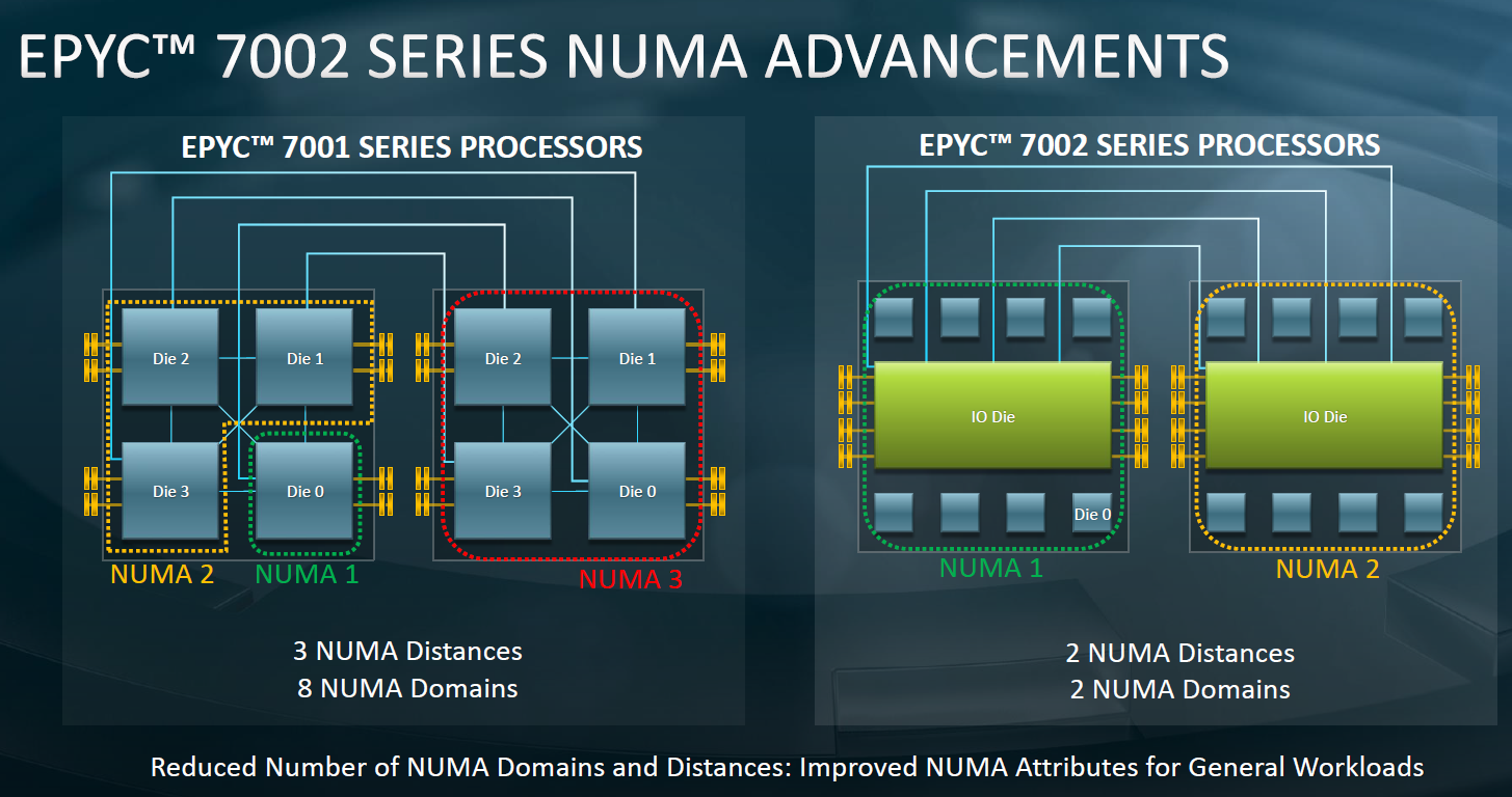
When we analyzed AMD's first generation of EPYC, one of the big disadvantages was the complexity. AMD had built its 32-core Naples processors by enabling four 8-core silicon dies, and attaching each one to two memory channels, resulting in a non-uniform memory architecutre (NUMA). Due to this 'quad NUMA' layout, a number of applications saw quite a few NUMA balancing issues. This happened in almost every OS, and in some cases we saw reports that system administrators and others had to do quite a bit optimization work to get the best performance out of the EPYC 7001 series.
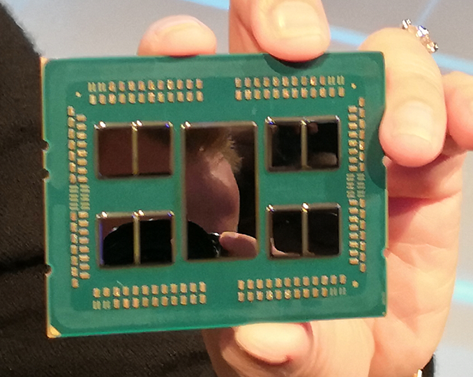
The New 2nd Gen EPYC, Rome, has solved this. The CPU design implements a central I/O hub through which all communications off-chip occur. The full design uses eight core chiplets, called Core Complex Dies (CCDs), with one central die for I/O, called the I/O Die (IOD). All of the CCDs communicate with this this central I/O hub through dedicated high-speed Infinity Fabric (IF) links, and through this the cores can communicate to the DRAM and PCIe lanes contained within, or other cores.
The CCDs consist of two four-core Core CompleXes (1 CCD = 2 CCX). Each CCX consist of a four cores and 16 MB of L3 cache, which are at the heart of Rome. The top 64-core Rome processors overall have 16 CCX, and those CCX can only communicate with each other over the central I/O die. There is no inter-chiplet CCD communication.

This is what this diagram shows. On the left we have Naples, first Gen EPYC, which uses four Zepellin dies each connected to the other with an IF link. On the right is Rome, with eight CCDs in green around the outside, and a centralized IO die in the middle with the DDR and PCIe interfaces.
As Ian reported, while the CCDs are made at TSMC, using its latest 7 nm process technology. The IO die by contrast is built on GlobalFoundries' 14nm process. Since I/O circuitry, especially when compared to caching/processing and logic circuitry, is notoriously hard to scale down to smaller process nodes, AMD is being clever here and using a very mature process technology to help improve time to market, and definitely has advantages.
This topology is clearly visible when you take off the hood.
Main advantage is that the 2nd Gen 'EPYC 7002' family is much easier to understand and optimize for, especially from a software point of view, compared to Naples. Ultimately each processor only has one memory latency environment, as each core has the same latency to speak to all eight memory channels simultanously - this is compared to the first generation Naples, which had two NUMA regions per CPU due to direct attached memory.
As seen in the image below, this means that in a dual socket setup, a Naples processor will act like a traditional NUMA environment that most software engineers are familiar with.
Ultimately the only other way to do this is with a large monolithic die, which for smaller process nodes is becoming less palatable when it comes to yields and pricing. In that respect, AMD has a significant advantage in being able to develop small 7nm silicon with high yields and also provide a substantial advantage when it comes to binning for frequency.
How a system sees the new NUMA environment is quite interesting. For the Naples EPYC 7001 CPUs, this was rather complicated in a dual socket setup:
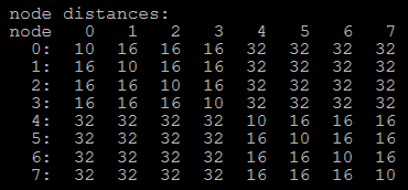
Here each number shows the 'weighting' given to the delay to access each of the other NUMA domains. Within the same domain, the weighting is light at only 10, but then a NUMA domain on the same chip was given a 16. Jumping off the chip bumped this up to 32.
This changed significantly on Rome EPYC 7002:

Although there are situations where the EPYC 7001 CPUs communicated faster, but the fact that the topology is much simpler from the software point of view is worth a lot. It makes getting good performance out of the chip much easier for everyone that has to used it, which will save a lot of money in Enterprise, but also help accelerate adoption.


180 Comments
View All Comments
JoeBraga - Wednesday, August 14, 2019 - link
It can happen if Intel uses the new archtecture Sunny Cove and MCM/Chiplet design instead of Monolithic DesignSanX - Thursday, August 15, 2019 - link
7zip is not a legacy test, it is important for anyone who sends big data over always damn slow network. Do you know all those ZIPs, GZs and other zippers which people mostly use, compress with turtle speeds as low as 20 MB/s even on supercomputers ? The 7Zip though parallelizes that nicely. So do not diminish this good test calling it "legacy"imaskar - Friday, August 16, 2019 - link
7zip is a particular program, doing LZMA in parallel, that's why it is faster that lets say gzip. But on server you often do not want to parallel things, because other cores are doing other jobs and switching is costly. There are a lot of compressing algorithms which are better in certain situations. LZMA rarely fits. More often it is it's LZ4 or zstd for "generate once, consume many" or basic gzip (DEFLATE) for "generate once, consume once". Yes, you would be surprised, but the very basic 30 years old DEFLATE is still the king if you care for sum of compress, send, decompress AND your nodes are inside one datacenter (which is most of the times).SanX - Thursday, August 15, 2019 - link
What you can say about Ian's own test he developed to demonstrate avx512 speed boost which shows some crazy up to 3-4x or more speedups ? Does your test of Molecular Dynamics tell that Ian's test mostly irrelevant for such huge improvement of speed of the real life complex programs?imaskar - Friday, August 16, 2019 - link
Probably because you can't use ONLY avx512. You still need regular things like jumps and conditions. And this is only the best case. Usually you also need to process part of the vector differently. For example, your vector has size 20, but your width is 16. You either do another vector pass, or 4 regular computations. Often second thing is faster or just the only option.realbabilu - Sunday, August 18, 2019 - link
Most of finite element software use Intel mkl to get every juice power spec of processor.it works for Intel ones not for amdAmd math kernel not heavily programmed, otnwaa just for Linux.
Other third party like gotoblas openblas still trying hard to detect cache and type for zen2.
I mean for workstation floating point still hard for amd.
peevee - Monday, August 19, 2019 - link
Prices per core-GHz:EPYC 7742 $48.26
EPYC 7702 $50.39
EPYC 7642 $43.25
EPYC 7552 $38.12
EPYC 7542 $36.64
EPYC 7502 $32.50
EPYC 7452 $26.93
EPYC 7402 $26.53
EPYC 7352 $24.46
EPYC 7302 $20.38
EPYC 7282 $14.51
EPYC 7272 $17.96
EPYC 7262 $22.46
EPYC 7252 $19.15
Value in this 7282 is INSANE.
peevee - Tuesday, August 20, 2019 - link
"Even though our testing is not the ideal case for AMD (you would probably choose 8 or even 16 back-ends), the EPYC edges out the Xeon 8176. Using 8 JVMs increases the gap from 1% to 4-5%."1%? 36917 / 27716 = 1.3319...
33%. Without 8 JVMs.
KathyMilligan - Wednesday, August 21, 2019 - link
University of Illinois Urbana-Champaign is very good university. I am too poorly prepared for this level of education. But I'm getting ready. I read a lot of articles and books, communicate with many smart former students of this university. I also buy research papers on site and this gives me a lot of useful information, which is not so easy to find on the Internet.YB1064 - Wednesday, August 28, 2019 - link
Looks like Intel has been outclassed, out-priced and completely out-maneuvered by AMD. What a disaster!