Examining Intel's Ice Lake Processors: Taking a Bite of the Sunny Cove Microarchitecture
by Dr. Ian Cutress on July 30, 2019 9:30 AM EST- Posted in
- CPUs
- Intel
- 10nm
- Microarchitecture
- Ice Lake
- Project Athena
- Sunny Cove
- Gen11
Intel has been building up this year to its eventual release of its first widely available consumer 10nm Core processor, codenamed "Ice Lake". The new SoC has an improved CPU core, a lot more die area dedicated to graphics, and is designed to be found in premium notebooks from major partners by the end of 2019, just in time for Christmas. With the new CPU core, Sunny Cove, Intel is promoting a clock-for-clock 18% performance improvement over the original Skylake design, and its Gen11 graphics is the first 1 teraFLOP single SoC graphics design. Intel spent some time with us to talk about what’s new in Ice Lake, as well as the product's direction.
The Core of Core: 10th Gen Core
Intel’s first batch of 10nm Ice Lake processors are being given the official brand name of ‘Intel 10th Generation Core’, and will feature up to four cores with hyperthreading and up to 64 execution units of Gen11 graphics. The aim of this first round of parts will be the thin-and-light mobile market in the form of the Ice Lake-U and Ice Lake-Y processors. Intel uses these designation for anything from 5W to 28W TDP, which covers all the mobile ultra-premium devices.
The cores inside Ice Lake-U are based on the ‘Sunny Cove’ microarchitecture, and are a further extension of the overall Core microarchitecture design. The new core affords several security benefits towards Spectre and Meltdown, and Intel is promoting a very healthy 18% IPC increase from its Skylake microarchitecture, which was initially launched as a 6th Gen Core part in 2015 (more on this later).
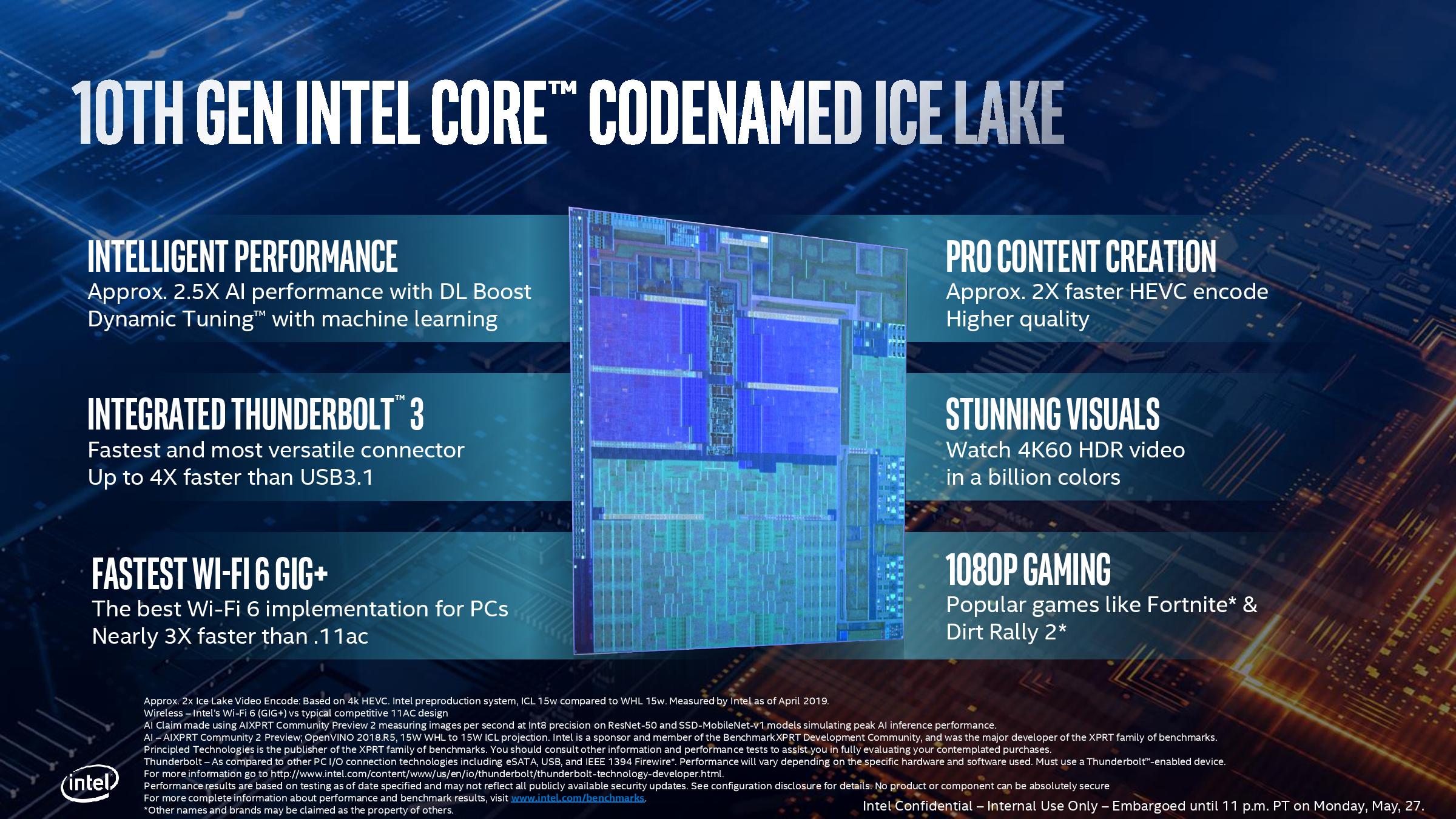
Asides from the core design, and the increased graphics performance, Intel is also putting a lot of effort into the rest of the design of the SoC. This includes AVX-512 extensions to help with deep learning and inference (applying pre-trained neural networks to new situations), integrated Thunderbolt 3 support for up to four full-bandwidth ports, CNVi support for Wi-Fi 6, and a range of platform designs under the umbrella of Intel’s new Project Athena initiative, which Intel hopes to spur on the next generation of premium devices and experiences in this market.
The Processors
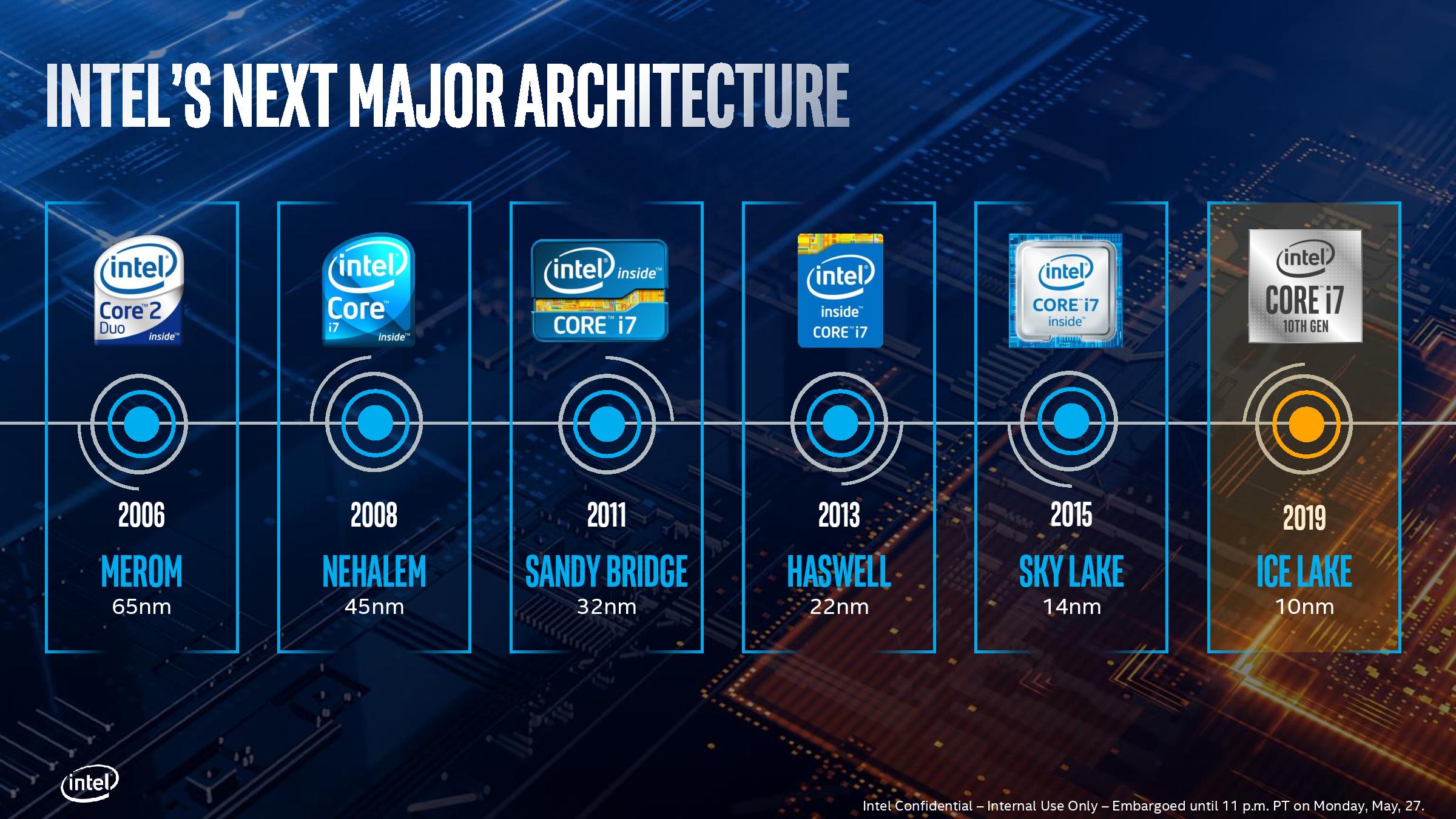
Despite Intel continually talking about upcoming devices, and very general top down specifications, we have not seen a full, official CPU list from the company about what frequencies and what performance metrics the new Ice Lake processors will have. At an event a couple of months back, Intel showed this slide:
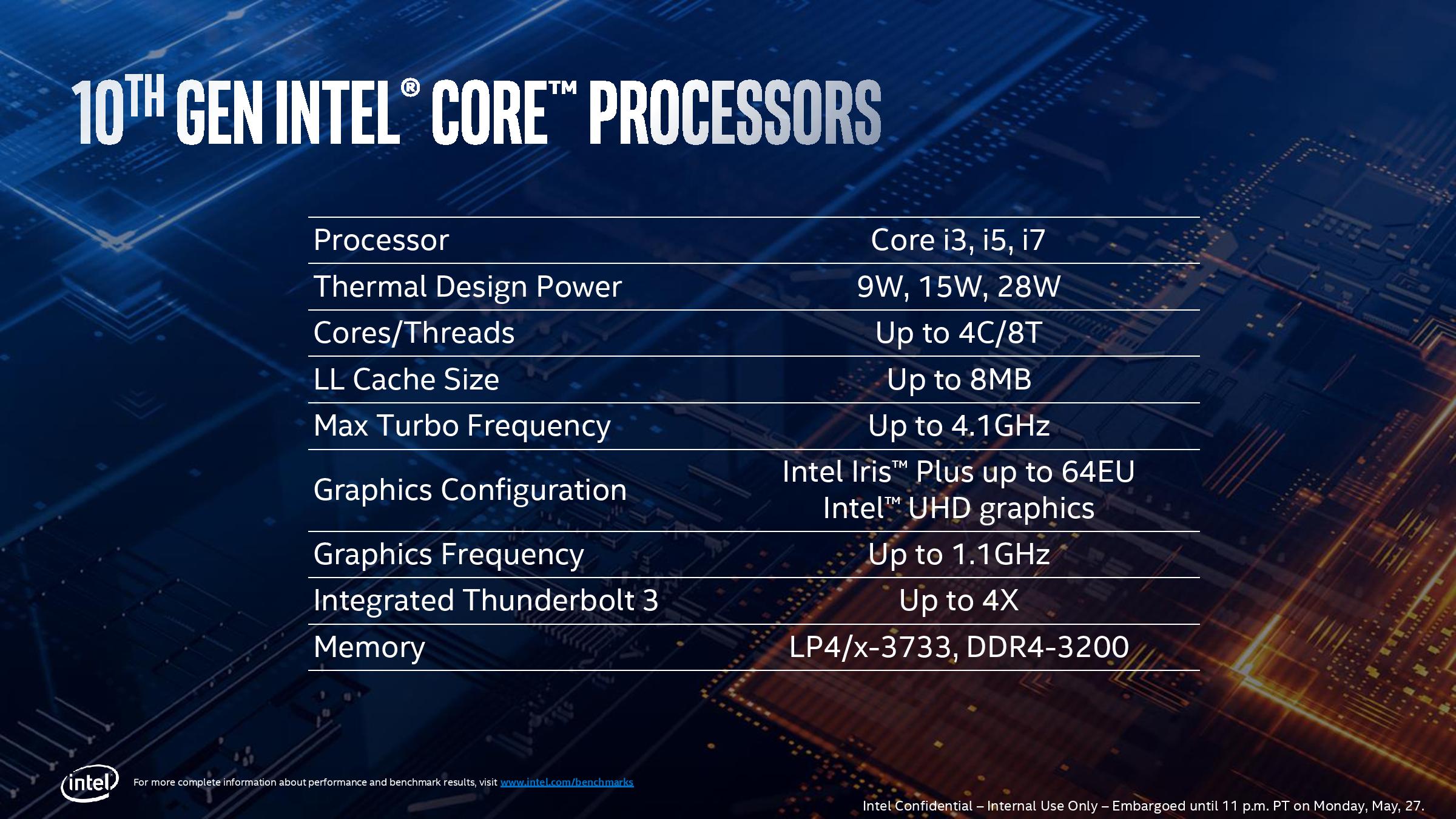
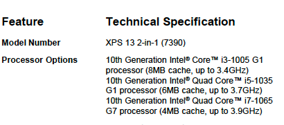
This slide states that we should expect to see i3, i5, and i7 versions of Ice Lake, with TDPs ranging from 9W to 28W, however the key value in there would be 15W. The processors will be up to four cores (so expect to see some dual cores), with a turbo frequency up to 4.1 GHz. Graphics will be available up to 64 execution units and up to 1.1 GHz, with certain platforms enabling four Thunderbolt 3 ports. Memory gets a healthy boost compared to previous platforms, with support being up to LPDDR4X-3733 (32 GB) or DDR4-3200 (64 GB). Each CPU has 16 PCIe 3.0 lanes for external use, although there are actually 32 in the design but 16 of these are tied up with Thunderbolt support.
Without a specific CPU list, it becomes a little worrying that the company hasn’t actually decided where the binning of these processors is going to fall. It also speaks to the fact that we are still several months away from having these processors in the market, so Intel is trying to find that balance of performance and yield. What we did discover at Computex earlier this year is that some vendors which are planning to have Ice Lake systems available, did disclose some CPU data:
There are of course some unconfirmed specification lists floating around the internet as well.
Ice Lake Design Wins, and Project Athena
At Computex, Intel showed off a number of systems it says will be the leading designs for Ice Lake in Q4. These included a very impressive Dell XPS 13 system, a HP design with a wooden finish, and an Acer Swift model aiming to be the lightest Ice Lake laptop to come to market.
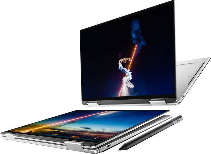
The Dell XPS 13
All of these devices come under Intel’s new Project Athena initiative.
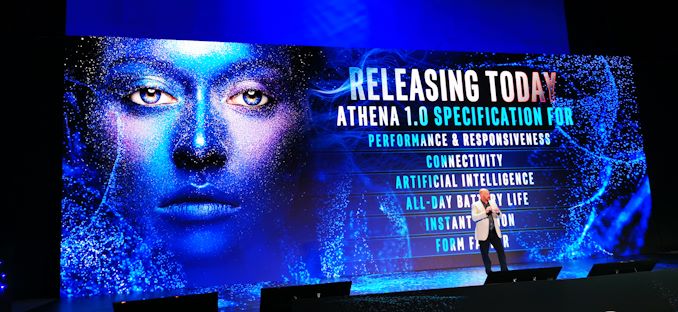
Project Athena borrows inspiration from Intel’s previous initiatives, such as Centrino and the Ultrabook. The goal here is to promote an ecosystem of Intel’s partners to design the next wave of devices and form factors that spurs on a good deal of innovation. This means that Project Athena has some very strict design targets that Intel’s partners have to follow and achieve in order to get the Athena designation/certification.

This means a lot of the following:
- Modern Connected Standby
- Biometric Login
- Wake from Sleep in <1 sec
- Core i5 or better
- >8GB DRAM in dual channel
- >256GB NVMe SSD, or Optane
- OpenVINO and WinML support
- 16+ hours of video playback
- 9+ hours of wireless web browsing
- Charge 4+hrs in 30 mins
- Thunderbolt 3, Wi-Fi 6, Gigabit LTE (optional)
- 2-in-1 or Clamshell,
- 12-15.6 inch, minimum resolution 1080p, touch display, narrow bezel on 3 sides
- Backlit keyboard, precision touchpad, pen support
Truth be told, supporting all of these means that the laptop should be a good buy with a decent user experience. These are a great set of goals to have for a mobile device, and it looks set that devices with the Athena designation should be very good.
However something to keep in mind is that in order to enable some of these technologies, it requires the OEMs to invest into Intel’s component ecosystem. Battery life, for example, helps if OEMs use the sub-1W panels that Intel has designated suitable for these devices. To implement Thunderbolt 3 and Wi-Fi 6 in a system is easy if a vendor uses an Ice Lake CPU, which also means that OEMs have to buy Intel’s AX200 chips (or a Killer AX1650, which is an AX200 underneath) to get Wi-Fi 6 to work. For Thunderbolt 3, re-timers are needed to support Type-C, and Intel makes those. The only other way to implement these features requires add-in cards which are higher power, and using those makes hitting the battery life targets, or the form factor requirements, difficult. Ultimately, to get the best of the Project Athena targets, the only way to do so is to buy more components from Intel or Intel approved component suppliers. Some may argue that programs like Project Athena end up cutting competition in this regard.
It should be noted that Ice Lake isn’t a requirement for Athena. But at this point it really, really, helps.
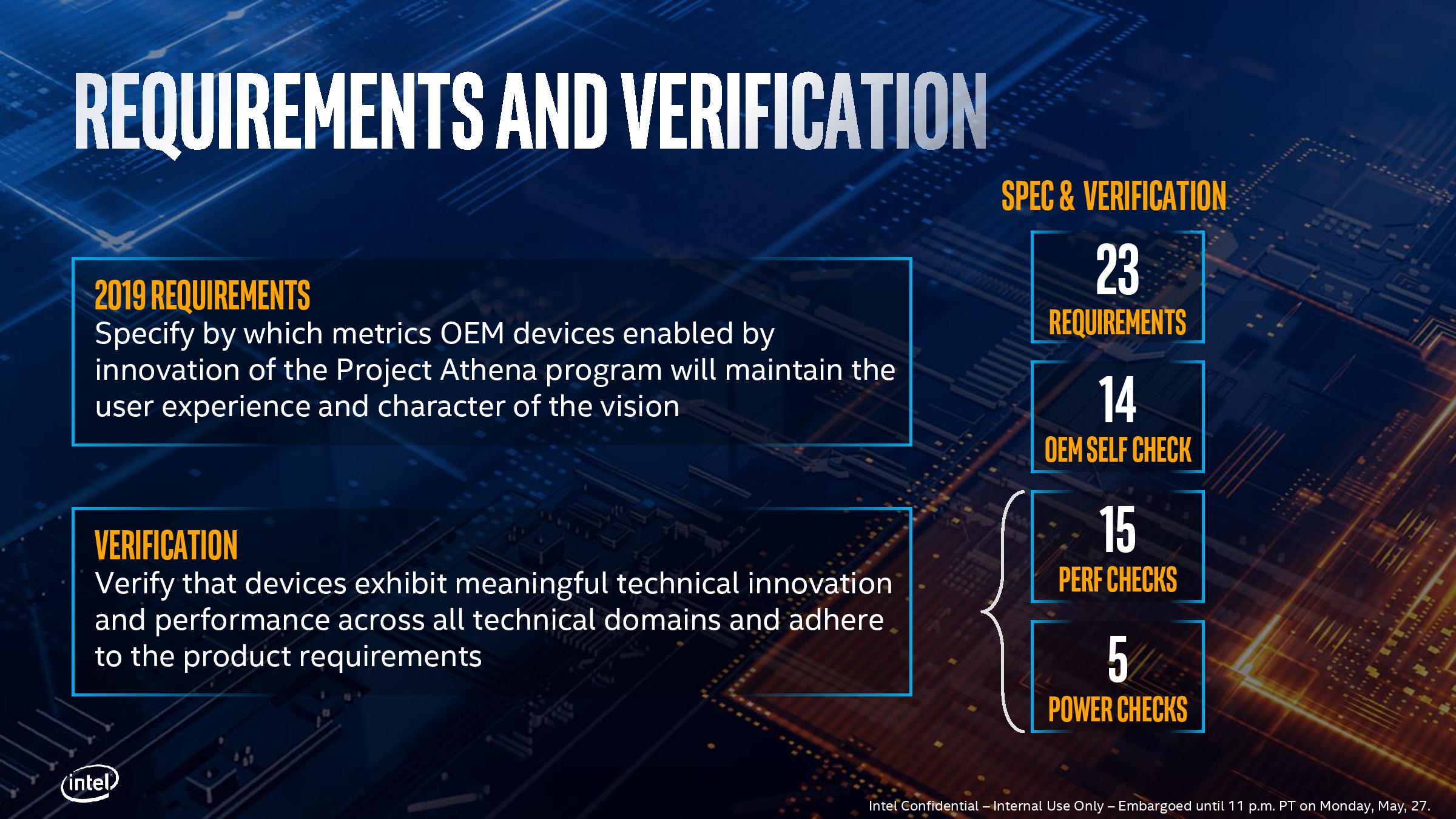
Intel will give the final Athena certification with a verification platform. This certification is built around what Intel says are ‘Key Experience Indicators’, such as the device being ready-to-go at a moment’s notice, providing enough worry-free battery life for common office tasks, and maintaining consistent responsiveness regardless of the state of the system.
Expect to see Athena devices in the market in Q4.
This Article
In this article, we’ll be going over Intel’s disclosures on Ice Lake, its new core Sunny Cove, as well as the new supported features and technologies within. We also comment on each of the new implemented items, with respect to user experience and realistic market/industry responses.


107 Comments
View All Comments
name99 - Wednesday, July 31, 2019 - link
That’s an idiotic chain of reasoning.ARM Macs will ship with macOS, not iOS. To believe otherwise only reveals that you know absolutely nothing of how Apple thinks.
As for comparison, the rough number is A12X gets ~5200 on GB4, Intel best (non-OC’d) gets ~5800. That’s collapsing lots of numbers down to one, but comparing benchmark by benchmark you see Apple does very well (almost matching Intel) across an awful lot.
If Apple can maintain its past pace (and there is no reason why not...) we can expect A13X to be anywhere from 20% to 35% faster, which puts it well into “fastest [non-OC’d] CPU on earth” territory for most single-threaded use cases. Can they achieve this? Absolutely.
Just process improvement can get them 10% frequency. I expect A13X to clock around 2.8GHz.
Then there is LPDDR5 which I expect they will be using, so substantially improved memory bandwidth. Then I expect they'll have SVE (2x256) and accompanying that basically double the bandwidth all the way out from L1 to DRAM.
These are just the obvious basics. There are a bunch of things they can still do that represent “fairly easy” improvements to get to that 25% or so. (These include more aggressive fusion, a double-pumped ALU, attached ALUs to load/store to allow load-ok and op-store fusion, a micro-op cache, long-term-parking, criticality prediction, ...)
So, if it’s so easy, why doesn’t Intel also do it? Why indeed? That’s why I occasionally post my alternative rant about how INTC is no longer an engineering company, it is now pretty much purely a finance company...
ifThenError - Friday, August 2, 2019 - link
Sorry, but both these comments seem mighty uninformed. The MacBooks Air and Pro currently and in the foreseeable future all run on Intel CPUs. The Apple Chips A12/13 are used in iPhone, iPad and the likes.And regarding your prediction, your enthusiasm seems way over the top. What are you even talking about? Micro-op cache on a RISC processor? Think again. Aren't RISC commands all micro ops already?
name99 - Sunday, August 4, 2019 - link
Strong the Dunning-Kruger is with this one...Dude, seriously, learn something about MODERN CPU design, more than just buzz-words from the 80s.
To get you started, how about you read
https://www.anandtech.com/show/14384/arm-announces...
and concentrate on understanding EVERY aspect of what's being added to the CPU and why.
Note in particular that 1.5K Mop cache...
More questions to ask yourself:
- Why was 80s RISC obsessed with REDUCED instructions?
- Why was ARM (especially ARMv8) NOT obsessed with that? Look at the difference between ARMv8 and, say, RISC-V.
- Why is op-fusion so important a part of modern high performance CPUs (both x86 and ARM [and presumably RISC-V if they EVER ship a high-performance part, ha...])?
- which are the fast (shallow logic, even if it's wide) and which are the slow (deep logic) parts of a MODERN pipeline?
ifThenError - Monday, August 5, 2019 - link
Oh my, this is so entertaining you should charge for the reading.You demand to go beyond just buzz words (what would be good) while your posts look like entries to a contest on how many marketing phrases can be fit into a paragraph.
Then you even manage to combine this with highly rude idiom. Plus you name a psychological effect but fail to transfer it to self-reflexion. And as cherry on the top you obviously claim for yourself to understand „EVERY aspect“ of a CPU (an unimaginably complex bit of engineering) but even manage to confuse micro- and macro-op cache and the conceptual differences of these.
I'm really impressed by your courage. Publicly posting so boldly on such a thin basis is brave.
Your comments add near zero information but are definately worth the read. Pure comedy gold!
Please see this as an invitation to reply. I'm looking forwards to some more of your attempts to insult.
Techgeek43 - Tuesday, July 30, 2019 - link
Fantastic article Ian, I for one, cannot wait for ice lake laptopsWonderful in-depth analysis, with an interesting insight into the Intel brand
repoman27 - Tuesday, July 30, 2019 - link
"The high-end design with 64 execution units will be called Iris Plus, but there will be a ‘UHD’ version for mid-range and low-end parts, however Intel has not stated how many execution units these parts will have."Ah, but they have: Ice Lake-U Iris Plus (48EU, 64EU) 15 W, Ice Lake-U UHD (32EU) 15 W. So their performance comparisons may even be to the 15 W Iris Plus with 64 EUs, rather than the full fat 28 W version.
I know you have access to the media slide decks, but Intel has also posted product briefs for the general public that contain a lot of this info: https://www.intel.com/content/www/us/en/products/d...
"On display pipes, Gen11 has access to three 4K pipes split between DP1.4 HBR3 and HDMI 2.0b. There is also support for 2x 5K60 or 1x 4K120 with a 10-bit color depth."
The three display pipes are not limited to 4K, and are agnostic of transport protocol—each of them can be output via the eDP 1.4b port, one of the 3 DDI interfaces which can support either DisplayPort 1.4 or HDMI 2.0b, or one of the up to 4 Thunderbolt 3 ports. Both HDMI and DP support HDCP 2.2, and DisplayPort also supports DSC 1.1. The maximum single pipe, single port resolution for HDMI is 4K60 10bpc (4:2:2), and for DisplayPort it's 4K120/5K60 10bpc (with DSC).
Thunderbolt 3 integration for Ice Lake-Y is only up to 3 ports.
abufrejoval - Tuesday, July 30, 2019 - link
What I personally liked most about the GT3e (48 EU) and GT4e (72 EU) Skylake variant SoCs was, that they didn't cost the extra money they should have, especially when you consider that the iGPU part completely dwarfs the CPU cores (which Intel makes you bleed for) and is much better than everything else combined together (have a look at the WikiChips layoutshttps://en.wikichip.org/wiki/intel/microarchitectu...
Of course, a significantly better graphics performance is never a bad thing, especially when it also doesn't cost extra electrical power: The bigger iGPUs might have actually been more energy efficient than their GT2 brethren at a graphics load that pushed the GT2 towards its frequency limits. And in any case if you don't crunch it on graphics, the idle consumption is near perfect: One of the reasons most laptop dGPU designs won't even bother to run 2D on the dGPU any more but leave that to Intel.
The biggest downside was that you couldn't buy them outside an Apple laptop or Intel NUC.
But however much Intel goes into Apple mode (the major customer for these beefier iGPUs) in terms of "x time faster than previous", the result aren't going to turn ultrabooks with this configuration into "THD gaming machines".
To have a good feel as to where these could go and whether they are worth the wait, just have a look at the Skull Canyon nuc6i7kyk review on this site: That SoC uses 72 EUs and 128MB of eDRAM and should put a pretty firm upper limit to what a 64 EU Ice Lake can do: Most of the games in that review are somewhat dated yet fail to reach 20FPS at THD.
So if you want to game on the device, you'd be much better of with a dGPU however small and chose the smallest iGPU variant available. No reason to wait, Whisky + Nvidia will do better.
If you want real gaming performance, you need to put real triple digit Watts and the bandwidth only GDDR5/6 or HBM can deliver to work even at THD, but with remote gaming perhaps it doesn't have to be on your elegant slim ultrabook. There again anything but the GT2 configuration is wasted, because only need the VPU part for decoding Google Stadia (or Steam Remote) streams, which is the same for all configurations.
For some strange reason, Intel has been selling GT3/4 NUCs at little or no premium over GT2 variants and in that case I have been seriously tempted. And only once I even managed to find a GT3e laptop once for a GT2 price (while the SoC is literally twice as big and the die carrier even adds eDRAM at zero markup), which I stil cherish.
But if prices are anywhere related to the surface area of the chip (as they are for the server parts), these high powered GTs are something that only Apple users would buy.
That's another reaons, I (sadly) don't expect them to be sold in anything bug Macs and some NUCs, no ChuWi notebooks or Mini-ITX boards.
abufrejoval - Tuesday, July 30, 2019 - link
...(need edit)Judging from the first 10nm generation, GPUs where the part where obtaining economically feasible yields didn't work out. Unless they have really, really fixed 10nm it's not hard to imagine that Intel could be selling high-count EU SoCs to Apple below cost, to keep them for another generation as flagship customer and perhaps due to long-term contractual obligations.
But maintaining GT2/3/4 price egality for the rest of the market seems suicidal even if you have a fab lead.
Not that I expect we'll ever be told: In near monopoly situations the so called market ecnomy becomes surprisingly complex.
willis936 - Wednesday, July 31, 2019 - link
What the hell is a THD in this context?jospoortvliet - Monday, August 5, 2019 - link
Probably full HD (True HD)?