Intel Unveils 10th Gen Core Ice Lake-U & Ice Lake-Y Mobile CPUs: 10nm Sunny Cove Later This Year
by Ian Cutress on May 29, 2019 8:00 AM EST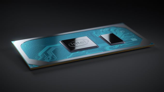
At Intel’s Keynote presentation here at Computex, the company finally lifted the lid on its first widely available new CPU design on its 10nm process, called Ice Lake. The official marketing name for these processors will be ‘Intel 10th Generation Core’, and will feature up to four CPU cores with Intel's new Sunny Cove architecture, new Gen11 graphics supplying up to 1TF of graphics/compute performance, and built in support for Wi-Fi 6 and Thunderbolt 3.
The story of Intel’s 10nm is a long and drawn out one, which we covered when we reviewed the first 10nm CPU, Cannon Lake, which only ended up in some limited Chinese system launch. Fast forward almost 2.5 years from when Intel officially announced it was shipping those 10nm CPUs and we have a full launch of Ice Lake, built on the company's greatly refined second-generation 10+ process. Intel spent a lot of its keynote presentation going through how it has driven the ecosystem and its ecosystem partners around developing systems with the new CPU in mind.
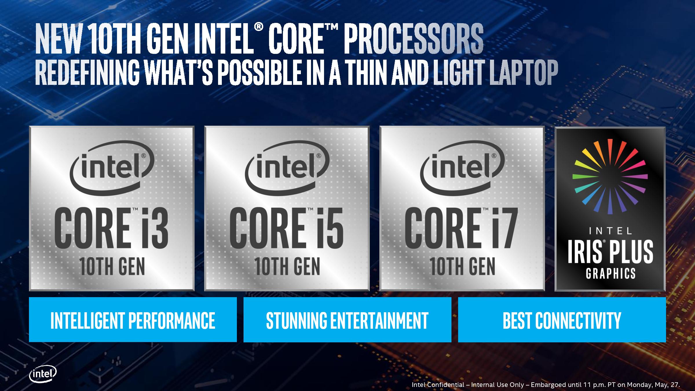
Intel is officially launching 11 different CPUs in the 10th Gen Core lineup, ranging from Core i3 to Core i7. Details on the specifications of those CPUs has not actually been released, which raises a number of questions of how much of a launch this actually is, however we do know that the best CPUs will have a turbo frequency up to 4.1 GHz and a top GPU frequency of 1.1 GHz. Users might consider this lower than 9th Gen mobile parts, which again raises questions. CPUs will be coming to market with 9W, 15W, and 28W variants.
Intel’s partners however have given us some specifications, and it shows in interesting adjustment in the naming scheme.
| OEM-Listed Intel Ice Lake 10nm CPUs | ||||||
| AnandTech | Core Threads |
Base Freq |
Turbo Freq |
IGP | TDP | Price (1ku) |
| i7-1065 G7 | 4C/8T | 1.3 GHz | 3.9 GHz | Yes | ? | ? |
| i5-1035 G1 | 4C/8T | ? | 3.7 GHz | Yes | ? | ? |
| i3-1005 G1 | 2C/4T | ? | 3.4 GHz | Yes | ? | ? |
At this point in time we’re not sure exactly what the ‘G7’ or ‘G1’ means in the name. It could be related to graphics, given that Intel will launch CPUs with 32 EUs, 48 EUs, or 64 EUs.
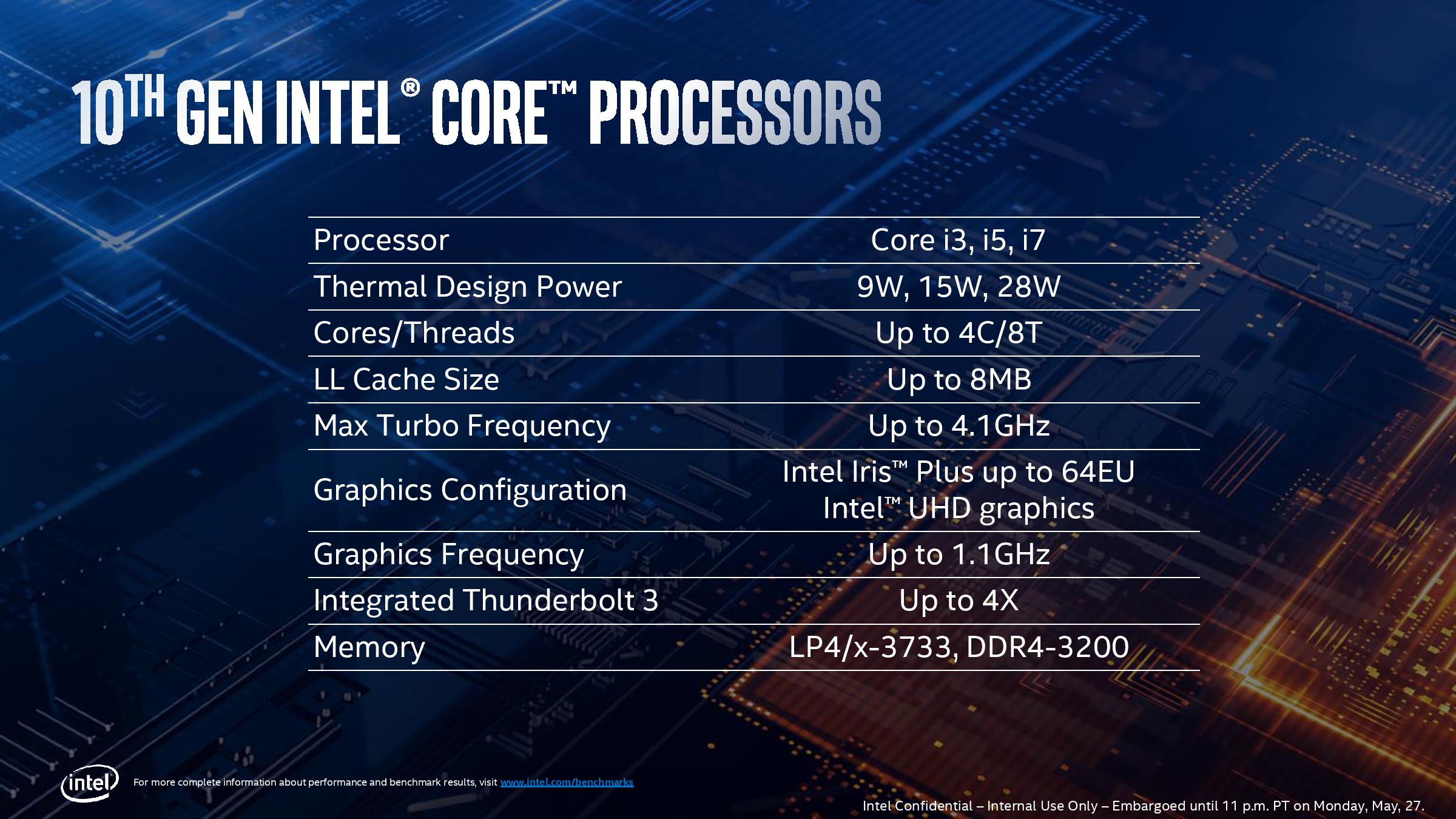
In accordance with their trio of TDPs, Intel has confirmed that there will be both Y-series and U-series Ice Lake parts. As a refresher, Intel's Y-series parts are their most compact, lowest-power chips, designed for passively cooled devices and other devices with limited cooling options, like 2-in-1s. Y-series chips have a nominal TDP of 9W – notably higher than the 5W TDPs for the current-generation Amber Lake-Y parts – and will be able to cTDP Up to 12W. Meanwhile Intel's U-series will, it appears, be the flag bearer for Ice Lake. These parts will have a nominal TDP of 15W, and can cTDP Up to 25W.
According to Intel's official product brief, both the U-series and Y-series parts will come with integrated GPUs with up to 64 EUs – this being particularly notable since the Y-series parts are going to be so low power. However it looks like Intel is going to split up the U-series a bit; 32 EU parts are listed as "Ice Lake U UHD", while 48 and 64 EU parts are "Ice Lake U Iris Plus". So Intel's Iris Plus branding will remain; and hopefully Iris Plus Ice Lake SKUs will be more common than today's Iris Plus parts.
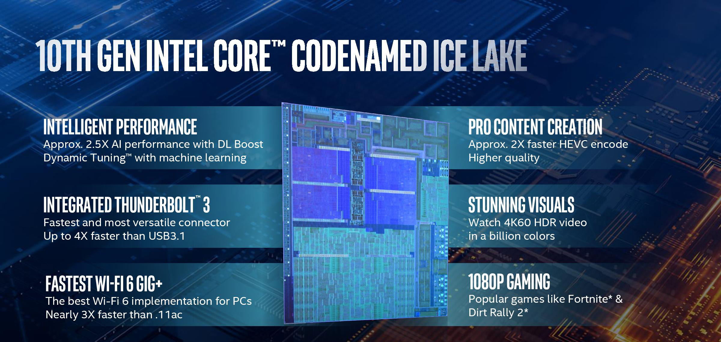
Intel has discussed Ice Lake to a certain degree back in December and more recently at a private event, which we will be publishing after Computex to give it the attention it deserves. But the new core is designed to have more execution units, wider out-of-order windows, better load/store functionality, a bigger cache arrangement, and Intel states that this is good for an average 18% raw clock-for-clock performance uplift compared to the original Skylake core released in 2016.
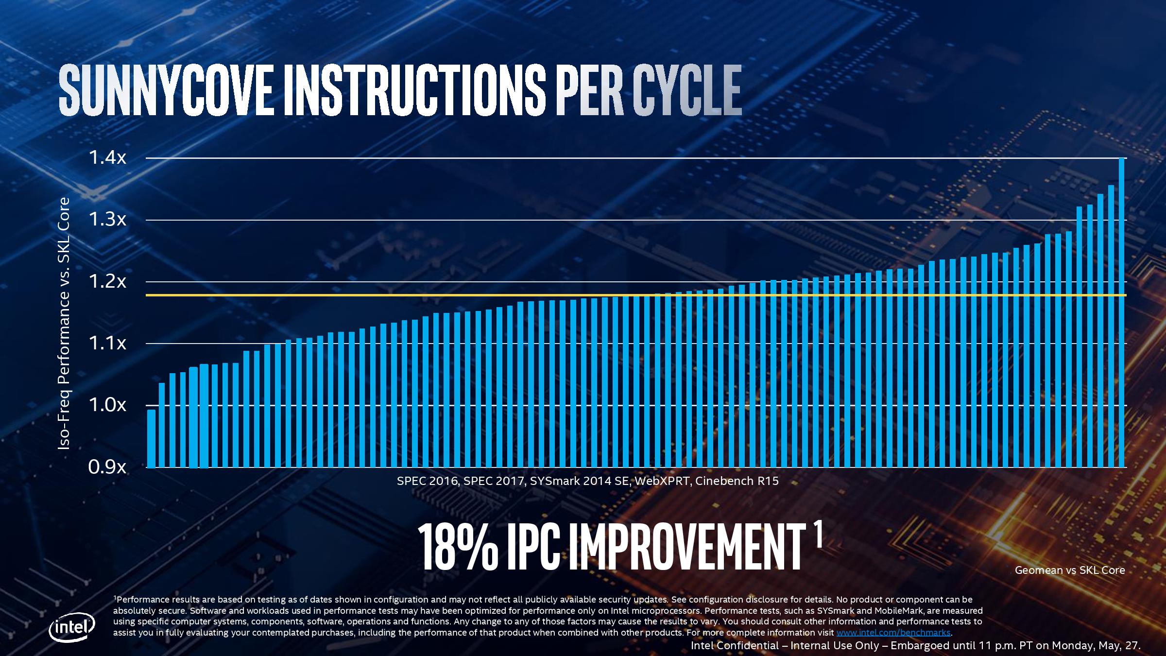
Users might be surprised about this 18% number, given that Intel has historically only provided low single digit boosts in recent generations. The reason for those single digit boosts comes down mainly to small parts of the core microarchitecture being widened. For Ice Lake, the doubling of the L2 cache, the increase in execution ports, and the dispatch capabilities of the front end of the core all provide big improvements. Intel also states that the pre-fetchers are improved, which also helps with that 18% IPC increase. It will be interesting to get hold of a system and to actually test/compare with Skylake, especially with all the security patches applied.
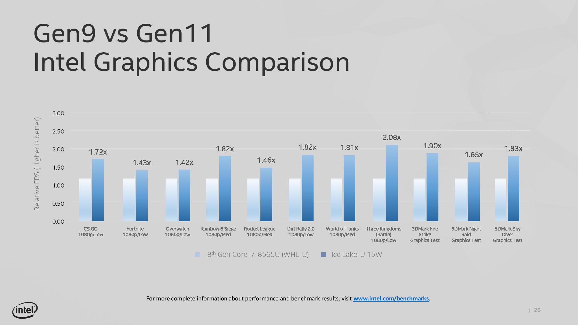
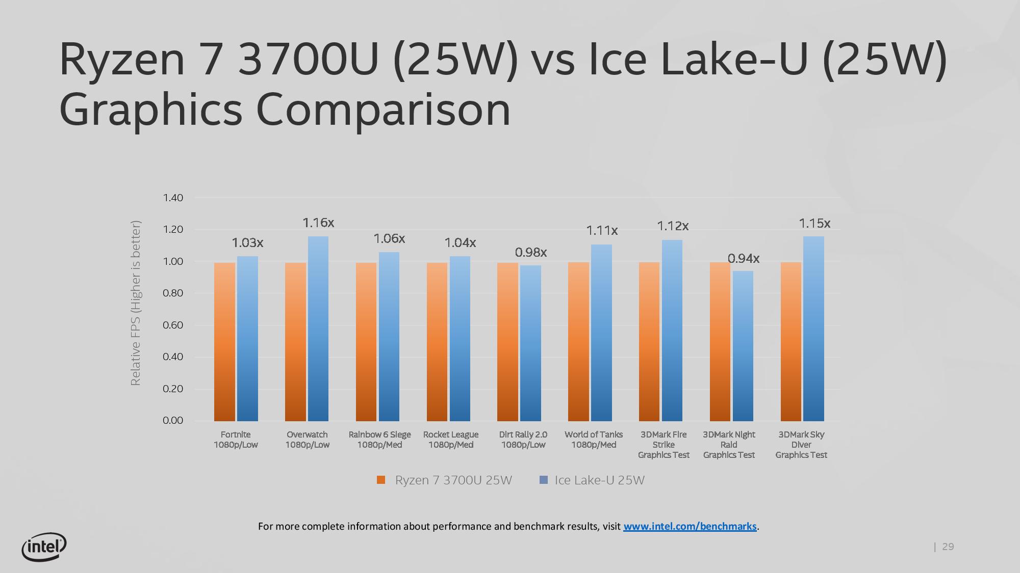
For graphics, Intel is stating that the best 10th Gen Core designs will be able to compete with what AMD has to offer with its mobile APU platforms. By increasing the number of execution units from 24 EUs to 64 EUs, Intel is promising over a 2x boost in graphics performance, which is facilitated by the better cache design on the CPU. The new graphics architecture, along with aggressive driver updates, should provide Intel better positioning in the thin-and-light gaming market. Benchmarks shown by Intel include many of the popular titles running today at 1920x1080 at either low or medium settings.
Core functionality aside, the new chips are also incorporating some of the latest I/O features. The biggest news here, of course, is integrated Thunderbolt 3 support for the on-chip 300 series mobile chip, finally doing away with the need for a separate PCIe-to-Thunderbolt controller. Not only will this save laptop OEMs space in their design, but as it's now a baseline feature of Intel's mobile chips, Thunderbolt 3 should become nearly ubiquitous across low-power laptops. Which considering that Thunderbolt 3 has been released to the world at large to be used as the basis for USB4, it's clear that Thunderbolt technology is quickly going to become a necessary feature for future laptops.
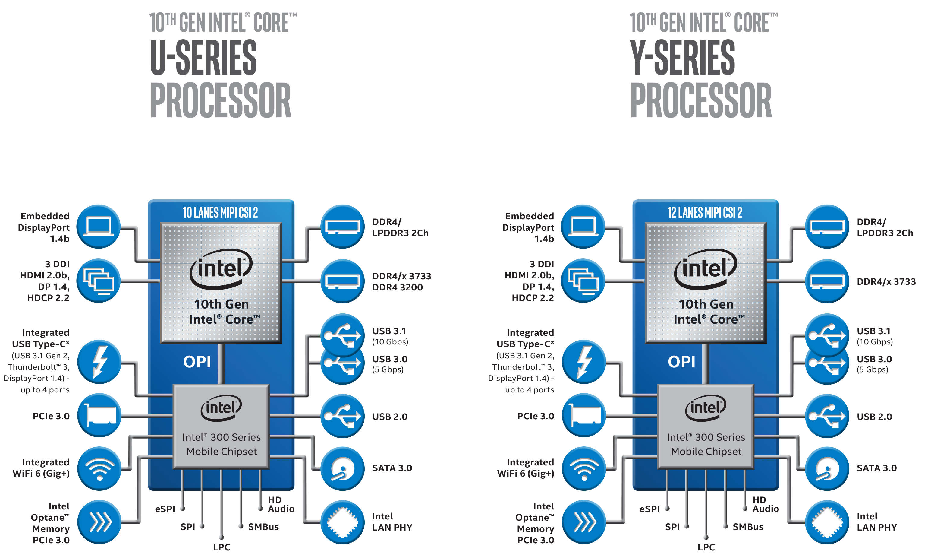
The other notable change here is support for Wi-Fi 6 (802.11ax), via Intel's increasingly well-established CNVi program. As with Intel's first-generation integrated Wi-Fi 5 functionality, Wi-Fi 6 is integrated in two parts. The Wi-Fi 6 Media Access Controller (MAC) is on Intel's chipset, meanwhile the RF hardware is on a separate companion module. Going this route is optimal for OEMs for regulatory reasons – the RF module can be certified separately – though it does mean they'll need to buy the RF module to make use of the processor's on-chip Wi-Fi capabilities. Interestingly, neither Intel nor the rest of the industry is wasting any time here; even though the Wi-Fi 6 standard hasn't been fully approved yet – it's still draft – it's already being integrated into hardware wide and far, including now mobile PC processors.
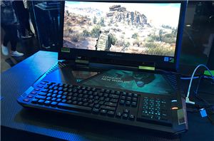
Overall, a number of ecosystem partners are at the Computex show with 10th Gen Core designs, including Dell, HP, Lenovo and others. For this new generation, Intel is also pushing its new Athena project, which we're covering in a separate article.
AnandTech's deep dive coverage of Intel 10th Gen Core will continue after Computex, with more details an analysis of the core microarchitecture. We're also working with Intel to get more access to Ice Lake platforms so we can provide a full testing profile of the new CPU family.
| Want to keep up to date with all of our Computex 2019 Coverage? | ||||||
 Laptops |
 Hardware |
 Chips |
||||
| Follow AnandTech's breaking news here! | ||||||


190 Comments
View All Comments
pk1489 - Thursday, May 30, 2019 - link
According the roadmap of intel(include some information by Huawei leaking ),intel will unveils cooper lake-sp in 2019q4 and unveils ice lake-sp in 2020q1 for datacenter. Those production will sell in 2020Q1.nonpracticingee - Thursday, May 30, 2019 - link
I find it astounding that so many commenters in a site like this do not understand rudimentary concepts. Let’s clarify a few things:IPC = instructions per clock cycle (instructions divided by cycle)
Frequency/clock speed = Cycles per second, measured in Hertz (cycles divided by second)
When determining which is faster, you can measure either:
1) Instructions processed in the same amount of time (where a higher number of instructions is faster)
In this case, we can calculate the instructions through:
X instructions = instructions/cycle * cycles/second * seconds
2) The time it takes to process the same set of instructions (where a lower duration is faster)
X seconds = instructions / (instructions/cycle * cycles/second)
Of course, since the above are being measured per core, the other variable you can modify is the number of cores:
X instructions = (instructions/cycle * cycles/second * seconds)/core * y cores
Given the geek bench scores posted earlier, we have the following:
Single core Whiskey Lake i7-8665u, cTDP up to 2.1GHz, boost 4.8GHz - 5341
Single core ICL i7-1065G7 cTDP up to 1.5GHz, boost 3.9GHz - 5234
Multicore Whiskey Lake - 16485
Multicore ICL - 17330
Single core IPC based on base clocks: ICL IPC is 37% higher
Single core IPC based on boost clocks: ICL IPC is 21% higher
Raw single core performance: ICL is 2% slower
Raw multicore performance: ICL is 5% faster
I don’t have the boost clock based on active cores table for ICL, so we can’t accurately extrapolate the data there. But based on base clocks, there is a 5% performance increase with 30% lower frequencies, meaning there is a remote possibility that clock for clock it’s 50% faster in multicore scenarios.
In reality, the figures obtained are a combination of the chips running at different frequencies and for the short duration that the Geekbench tests run, the chips will primarily run close to the top rated boost clock speeds.
The IPC number is higher than what Intel is claiming because the work load that the CPU architects chose to model while designing the microarchitecture is different from what Geekbench is using. Based on the figures from the computed IPC based on boost clocks, they are similar though. The modifications they make to the microarchitecture are informed by the work loads they choose and there may be regressions in some work loads if they consider the improvements in other work loads to be more valuable.
Note: This only applies when comparing the same set of instructions. If the instruction set architecture (or even just the instructions used, like vectorized vs scalar instructions) is different, then the number of instructions processed is not equal to the amount of work done. E.g. if in one chip with one ISA, the same logical operation requires 1 instruction to perform that takes 6 cycles (IPC is 1/6), while another chip with a different ISA requires 3 instructions that take 2 cycles each (IPC is 1/2), the second chip has a higher IPC but in terms of actual work done, they are identical.
Both Intel and AMD implement the same ISA (with a few differing instructions) and thus can be directly compared for the most part. Recall that when AMD and Intel were competitive in the early 2000’s, Intel heavily marketed their higher frequencies and AMD named their Athlon XPs with names that didn’t represent the CPU frequencies because they had lower frequencies but higher IPC. AMD provided better value then, and with Ryzen 3, will appear to do the same again for the desktop market.
To generalize the Intel chips we’ve seen over the past few years we have:
Sandy Bridge
Ivy Bridge = Sandy Bridge + better GPU + 22nm
Haswell
Broadwell = Haswell + 14nm
Skylake
Kaby Lake = Skylake with higher frequencies
Coffee Lake = Skylake with higher frequencies, with more cores
Coffee Lake Refresh = Skylake with higher frequencies, with more cores, with more cores
What Intel was targeting to have is:
Sandy Bridge
Ivy Bridge = Sandy Bridge + better GPU + 22nm
Haswell
Broadwell = Haswell + 14nm
Skylake
Cannon Lake = Skylake + AVX512 + new memory module + 10nm
Ice Lake
In the amount of time between Skylake and Ice Lake, Intel could have finished development and begun shipment of yet another microarchitecture (beyond Ice Lake). However, because Intel’s microarchitectures are tightly coupled with a process node and Ice Lake was designed with the 10nm libraries, Intel could not produce chips with a new microarchitecture in 14nm. Since they are using the same microarchitecture and, thus, had constant IPC, the only remaining variables they could change to improve performance are: A) the frequency, and B) the number of cores. Kaby Lake modified variable A, Coffee Lake and Coffee Lake Refresh, modified A and B.
From the power usage perspective, we have the following:
1) shorter amount of time to perform the same work load, given higher frequencies and more cores
2) longer amount of time CPU spends idle thus longer amount of time in low power states
3) higher peak power usage because of more cores running at the same time
4) lower average power usage because CPU is idle longer
This plays a large part in Intel’s logic of keeping the TDP number identical. Obviously, if they defined TDP to represent peak power usage, it isn’t possible to keep the same figure if you have more cores running with mostly the same manufacturing node. If a core requires 2W to run, logically, running 2 cores will not also only require 2W at the same node.
Because the 10nm launch is so delayed and we’ve had Coffee Lake, et al to compensate, we have the following effect: die sizes are larger, but wafer sizes are the same. This means fewer chips per wafer, and thus lower capacities. Add to that binning for products like the 9900KS, and we have to go through multiple wafers to win the silicon lottery and get dies that can be placed in halo products. This in turn affects supplies to customers, where Intel wasn’t able to cope with the demand. This has caused Intel to invest in more 14nm fabs. This will likely cause Intel to produce more 14nm products for an even longer duration to make up for the costs of investing into more 14nm fabs.
Once Intel decided it would move away from the Tick-Tock strategy and embrace Process + Architecture + Optimization, they told us that 10nm would have lower performance than 14++ and 10+ would be roughly equivalent to 14++. This appears to be because 14+ and 14++ products allowed high frequencies that 10+ products are compensating for through higher IPCs. It is easy to see why Cannon Lake became a non-starter. The same IPC with lower clocks meant lower performance per core and low yields meant you had to keep the die size tiny (and consequently core count low) to have a viable die. Fewer cores, lower frequencies, and high costs means Cannon Lake was always going to be a disaster by the time we got Coffee Lake. Ice Lake with its higher IPC is able to compensate for the lower frequencies to provide comparable performance. The marketing for Ice Lake is touting Gen11 graphics and improvements to the platform because the CPU performance is essentially identical due to the less mature node.
TLDR
IPC gains are not hogwash. Intel is comparing ICL to SKL because Intel has ONLY been shipping SKL variants for 4 years now. In fact, IPC gains are the only reason Intel can afford to ship 10nm products now from a user perspective.
ICL will perform slightly slower for single threaded applications because of lower clocks but perform slightly faster for multithreaded workloads because IPC gains compensate for the lower clocks.
This doesn’t mean ICL itself underperforms. It’s currently hamstrung by the maturity of the node.
Hixbot - Thursday, May 30, 2019 - link
Wow, excellent post. I saw how much text and almost didn't read. but glad I did read it. Thanks.Rudde - Thursday, May 30, 2019 - link
Is it reasonable to count AES and AVX-512 to Ice-lakes advantage? Ice-lake has better AES acceleration (21%ST/ 33%MT improvement in Geekbench compared to i7-8665U). Ice-lake gets a boost in GEMM and FFT from AVX-512 (curiously it performed worse in ST GEMM than i7-8665U).My point is that support for specialised code improves the score of the Ice lake, making a general comparision harder. It is a nice boost in workloads that support it, but those are few and far between at the moment. It is also worth pointng that AVX instructions doesn't run at the same clock speed as integer instructions.
nonpracticingee - Thursday, May 30, 2019 - link
I wouldn't say they're unreasonable if they accelerate common workloads. Intel's been marketing how its specialized instructions improve performance since MMX. AMD's done the same thing with 3DNow! On that note, I don't think Intel's leaning heavily on AVX-512 for their IPC improvement claims. The product brief they released has a disclaimer about AVX lowering clock speeds and people have reported that AVX-512 is causing their CPUs to throttle, slowing down execution of even non-AVX code. If thermal issues are still a problem with AVX-512, they're probably amplified in Ice Lake because of the smaller die sizes. It's harder to dissipate heat when the surface area is smaller. Hopefully Ian can score some samples soon and we'll get to see real results. If anything, cache improvements and a better back end probably account for most of the IPC gains. We've seen what wonders that does for every generation of Apple A chips. Again, I'm eager to see what Ian has to share.zodiacfml - Thursday, May 30, 2019 - link
Yes. I guess we just have younger readers and don't understand what is going on with Intel. Aside from that, we haven't seen proper reviews yet and AMD will delay 7nm mobile. IceLake is important, though I don't like specs for the i3 chip with only two cores.Targon - Friday, May 31, 2019 - link
No delay from AMD on laptop chips, but AMD always starts with high end desktop to get the chips into systems quickly. If AMD is planning on Navi going into the 7nm laptop chips for the next generation, making sure that the GPU drivers work will be good for OEMs as well. The question is when AMD will release the new laptop chips. AMD released the 3000 series laptop chips(based on 12nm Zen+ and Vega) in January of 2019. If AMD gets the next generation out in November of 2019, that would be a positive thing.Targon - Friday, May 31, 2019 - link
A big factor that makes the stated numbers more of a challenge is security mitigations, and not having all mitigations in place when Intel stated the +18% IPC figure. This implies that the +18% figure isn't going to be accurate once the mitigations are in place. Most people are not saying that there are no improvements, but are pointing out that the actual IPC improvement may be completely offset by security mitigation numbers combined with lower chip frequencies. To make it even more difficult, Intel is known for setting TDP figures that only apply to the base frequency. If base frequency is only 1.1GHz for a 15W TDP chip, and that 15W is only accurate at the base frequency, then is Intel actually doing well compared to an AMD Ryzen 5 3500U or Ryzen 7 3700U in laptop performance?nonpracticingee - Friday, May 31, 2019 - link
You're right that _some_ of the comments were theorizing that the security mitigations account for most of 18% figure. I've previously responded to some of those comments to point out that the Geekbench numbers quoted are from Whiskey Lake and Ice Lake. _Both_ have some security mitigations in hardware. As I mentioned in my post, you'll see an IPC improvement higher than what Intel claimed because of a difference in the workload being tested. I did, however, also mention that there's barely any improvement visible when looking at the raw performance because of the low frequencies. This is why I said the IPC gains are the only reason Intel can afford to ship 10nm products. They can't sell something that performs worse but they also can't market single digit performance improvements and slight regressions so they focus on the GPU and platform improvements.The main reason I posted anything at all is because it's frustrating to see that people don't have a clue what IPC means. While _some_ of the posts brought up spectre/meltdown/mds, a lot of the others appear to think that each set of chips Intel has released over the past 4 years had IPC gains. I explained that Intel had to keep the IPC constant and rely on the two other factors they could change to improve performance: a) frequency, and b) core count.
In terms of laptop performance, it'll be hard to get a fair comparison regardless because OEMs tend to put AMD chips in cheap laptops with low end specs. Ice Lake does have a process advantage over the mobile Ryzen 3 chips since those are still manufactured at the 12nm node. We'll need to wait for reviews of actual products to see the difference. Moreover, the overall platform is a bigger deal in mobile products because of battery life concerns. In terms of laptop energy consumption, it isn't just the CPU that matters. Intel has integrated the functionality of more chips into its new PCH. This means that there will be fewer chips, lower overall power draw, smaller motherboard footprints, and lower costs for manufacturers. Integrating WiFi and Thunderbolt into the PCH alone would save a considerable amount of power.
tipoo - Monday, June 3, 2019 - link
Yup. I'm surprised so many in the AT audience don't understand this. IPC has been the same since Skylake, it's the clock speeds/boosts that have risen, so 18% over Skylake is very nearly 18% over everything since on Instructions Per Clock.