Gordon Moore’s Desk at Intel: 50 Years of Silicon Wafers
by Ian Cutress on May 30, 2018 9:00 PM EST- Posted in
- CPUs
- Intel
- DRAM
- Moore's Law
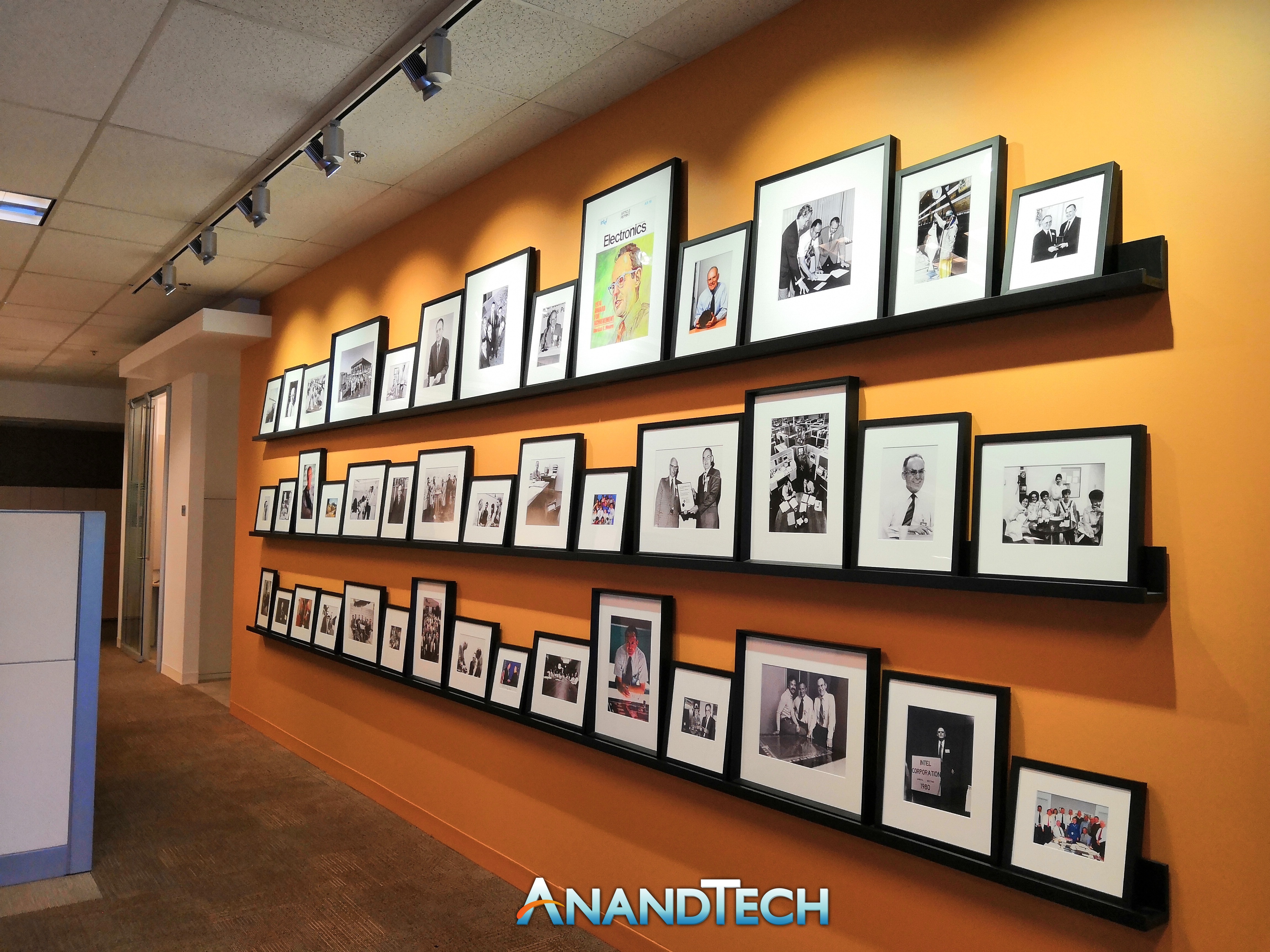
Today was Intel’s Data Center Tech Summit, where the first Optane-based memory modules are officially disclosed, although a full launch is set for later this year. The Summit did not take all day, and our contacts at Intel offered to show us the desk of the eponymous Gordon Moore, co-founder and chairman emeritus of Intel. As described, it sits as he likes it, among a number of other Intel employees next to the window, but relatively unchanged across site renovations. For us, it was the wafers on display that showcase his place in the semiconductor space as one of the most important people that have ever been in this industry.
Moore’s Law, followed by Moore’s Desk, and Moore's Wall
In 1965, Gordon Moore coined a phrase that later became Moore’s Law, stating that the number of components (transistors) in a circuit doubles every 12 months. This was later revised to 24 months in 1975. The phrase has been a mainstay when discussing the newest generation of hardware, and the plaques on display around the desk it is clear to see why.
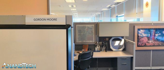
Taking our image at the top here, his cubicle is open plan with the rest of the workspace, albeit a little bigger than most other employees.

On the far right is a framed photo, showing Moore holding up a life size representation of a die layout.

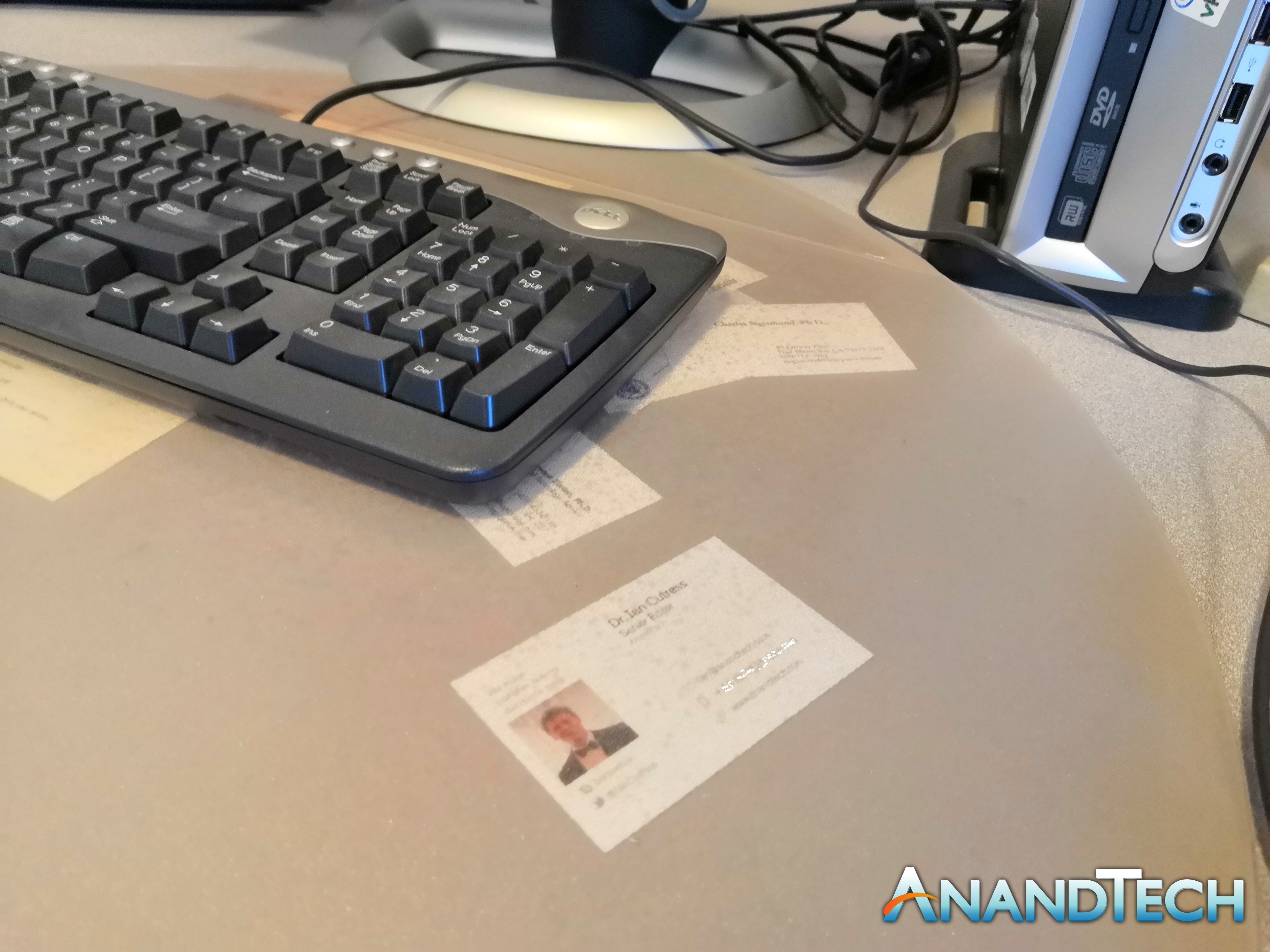
The desk itself is different to the others – other employees seem to have adjustable motorized height desks and chairs, while Moore’s is pretty static. The desk is clean, although an array of business cards from other people sits underneath the transparent mouse mat that surrounds the immediate area in front of the share.
There’s no super Intel workstation and 4K widescreen monitor setup here, it looks like a simple mainstream system with a vPro enabled processor and an old school 5:4 monitor.
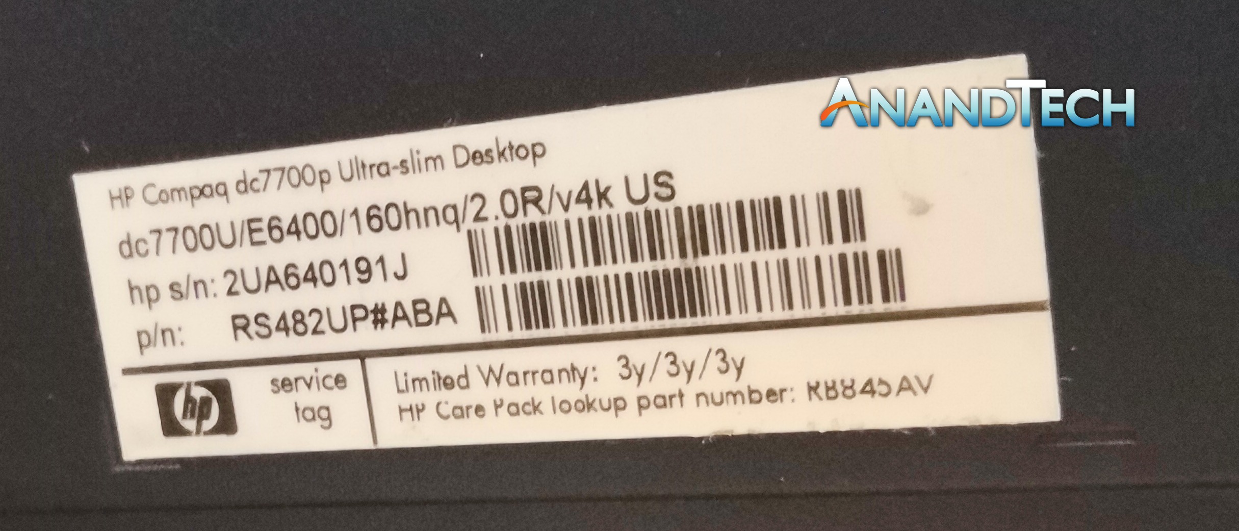
On closer inspection, it is a vPro-enabled Core 2 Duo E6400 system.
To the left, right, front, and behind, are a series of plaques and accolades.
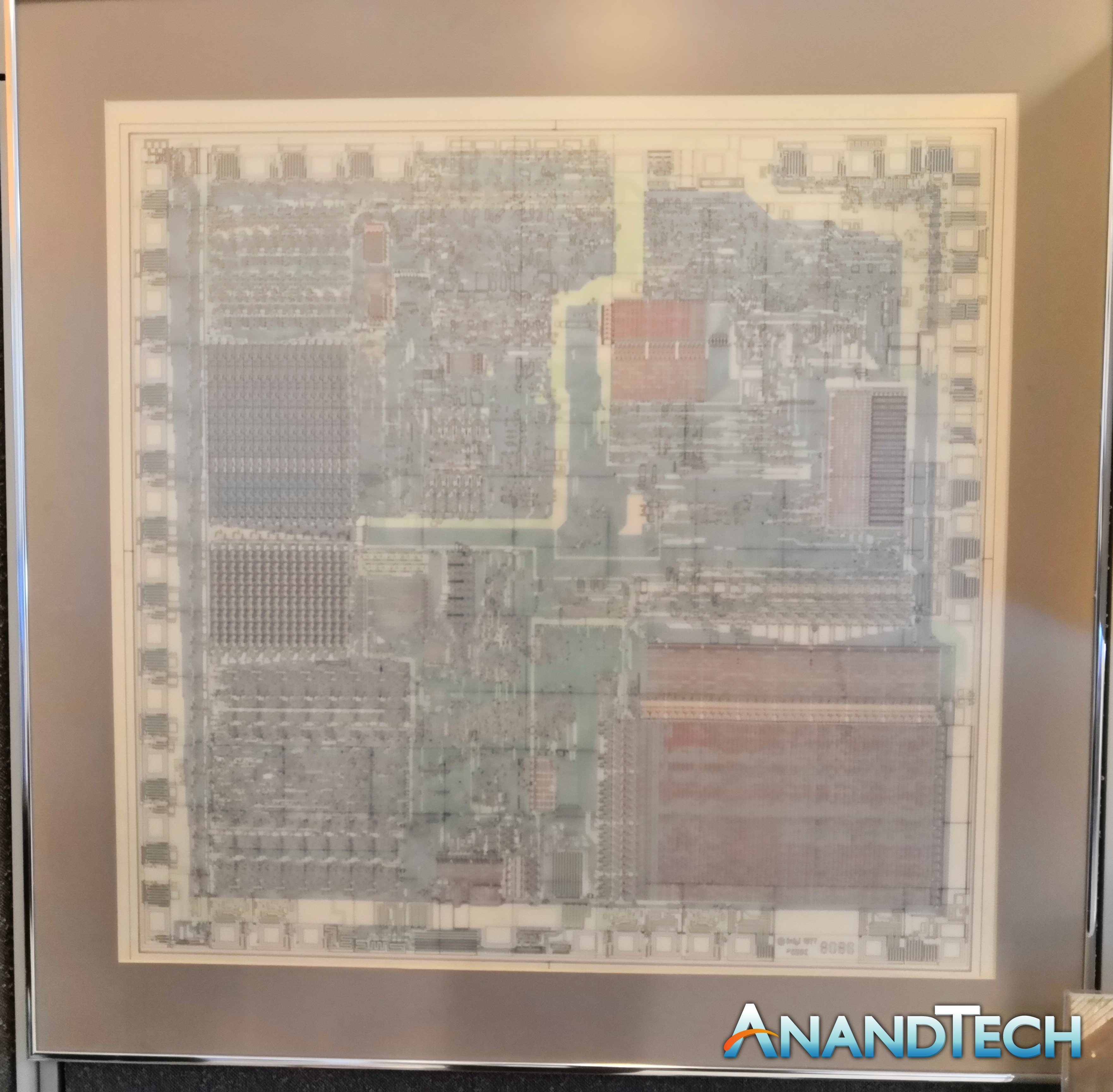
On the wall to the immediate right is one of the special items of the industry: a circuit diagram of Intel’s original 8086 processor from 1977. If anyone was going to have this image next to them while they sat at the desk, it would have to be Gordon Moore.
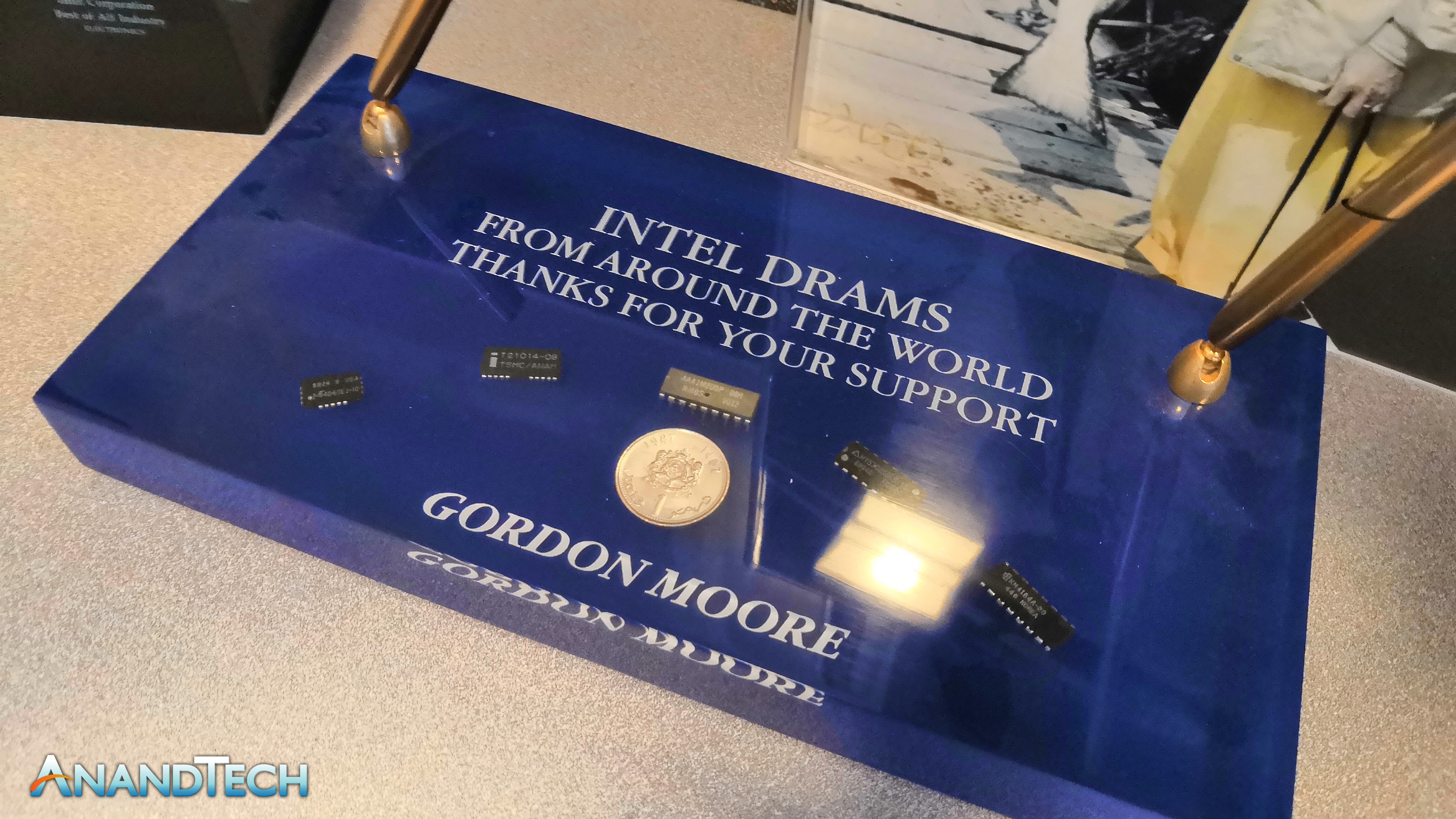
Directly underneath the 8086 image is a paperweight with the hardware that Intel originally built: DRAMs. Intel was a DRAM company, and here are a few old chips dating back to the early days of the company. Date codes on these chips are unknown, but we can clearly see ‘Korea’ and ‘TSMC’ listed on a couple of them.
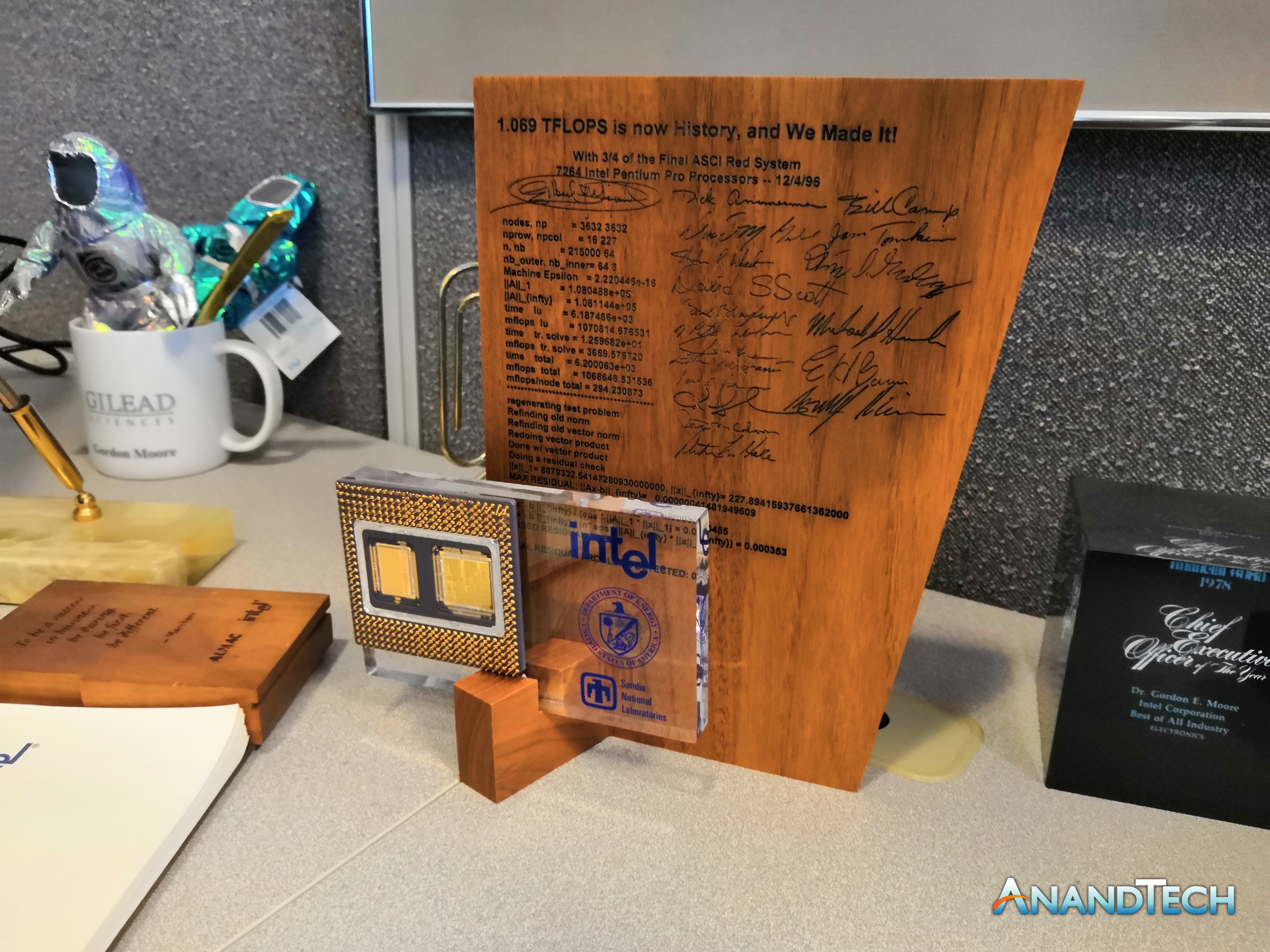
Next to this and sitting to the right of the PC is an award to represent the processor used in the first teraflop supercomputer: Intel’s Pentium Pro from April 1996. The design from Sandia National Laboratories includes the chip in perspex along with performance numbers and signatures from the members of the team. If we look closely at the chip, we can see some of the pins have certainly been nudged and bent.

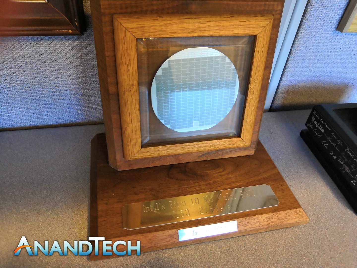
The nearest wafer to Moore’s chair is one from January 1982, showing Intel’s first 10 megabit wafer of RAM. We can tell that there are 13 dies across the center and 11 dies from top to bottom, with a few missing, but all from a 150mm wafer.
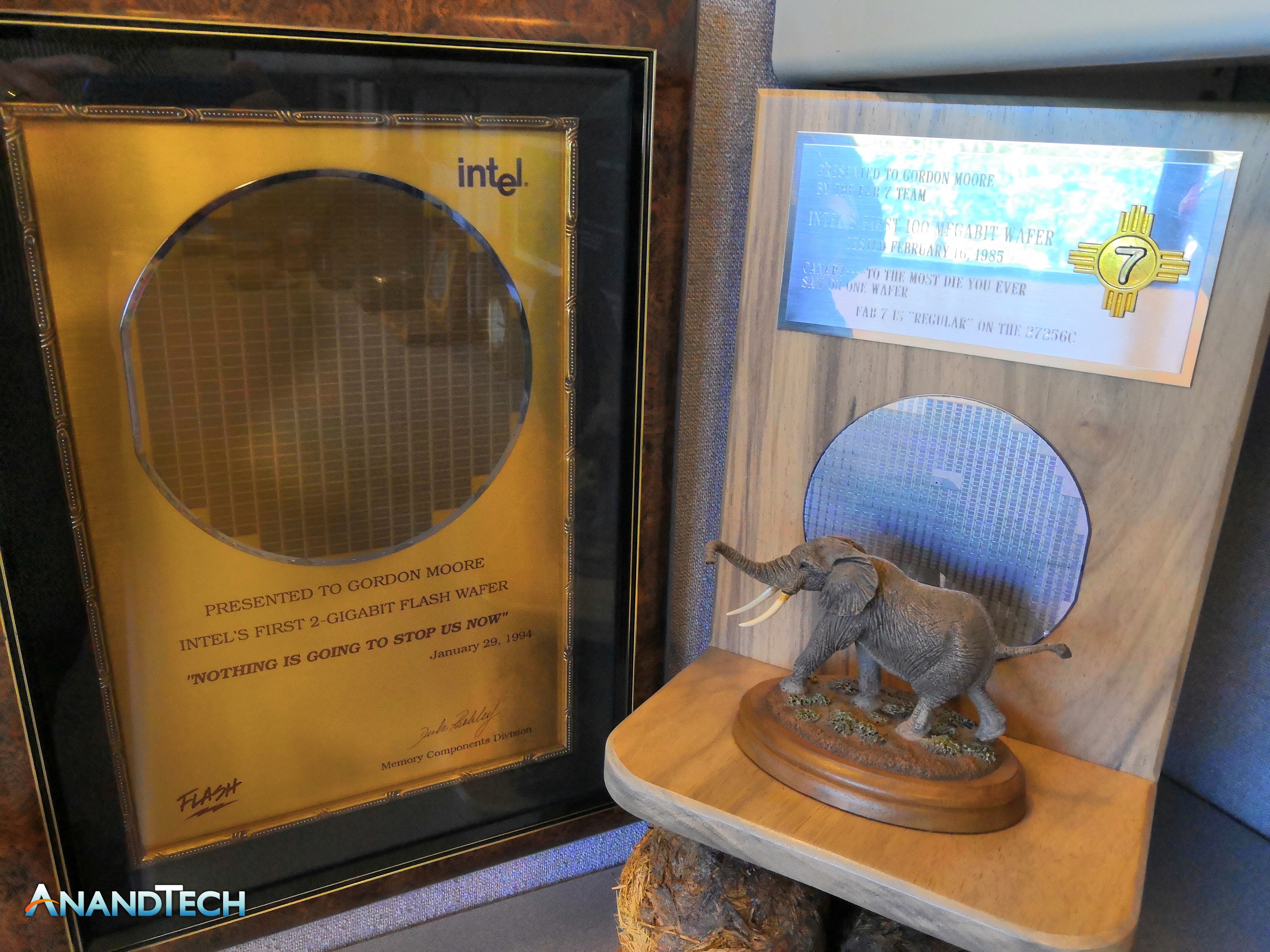
The progress from 1982 to 1985 to 1994 was moving from a 10 megabit wafer to a 100 megabit wafer then a 2 gigabit wafer, although this time on Flash. The wafer on the right is the 100 megabit wafer, and reads the words ‘to the most die you ever saw on one wafer’. By 1994, the wafers were moved up to 200mm.

Behind the desk is a small meeting table and a wall covered in wafers, which shall now be called Moore’s Wall of Wafers. There are too many individual bits of history here to go through them all, however I picked out a few milestones and interesting parts.
![]()
This one is perhaps a really important milestone for Intel: the first million transistor microprocessor. This was the 80860 from September 1988, as shown on the tiny wafer, measuring 9x13 dies.
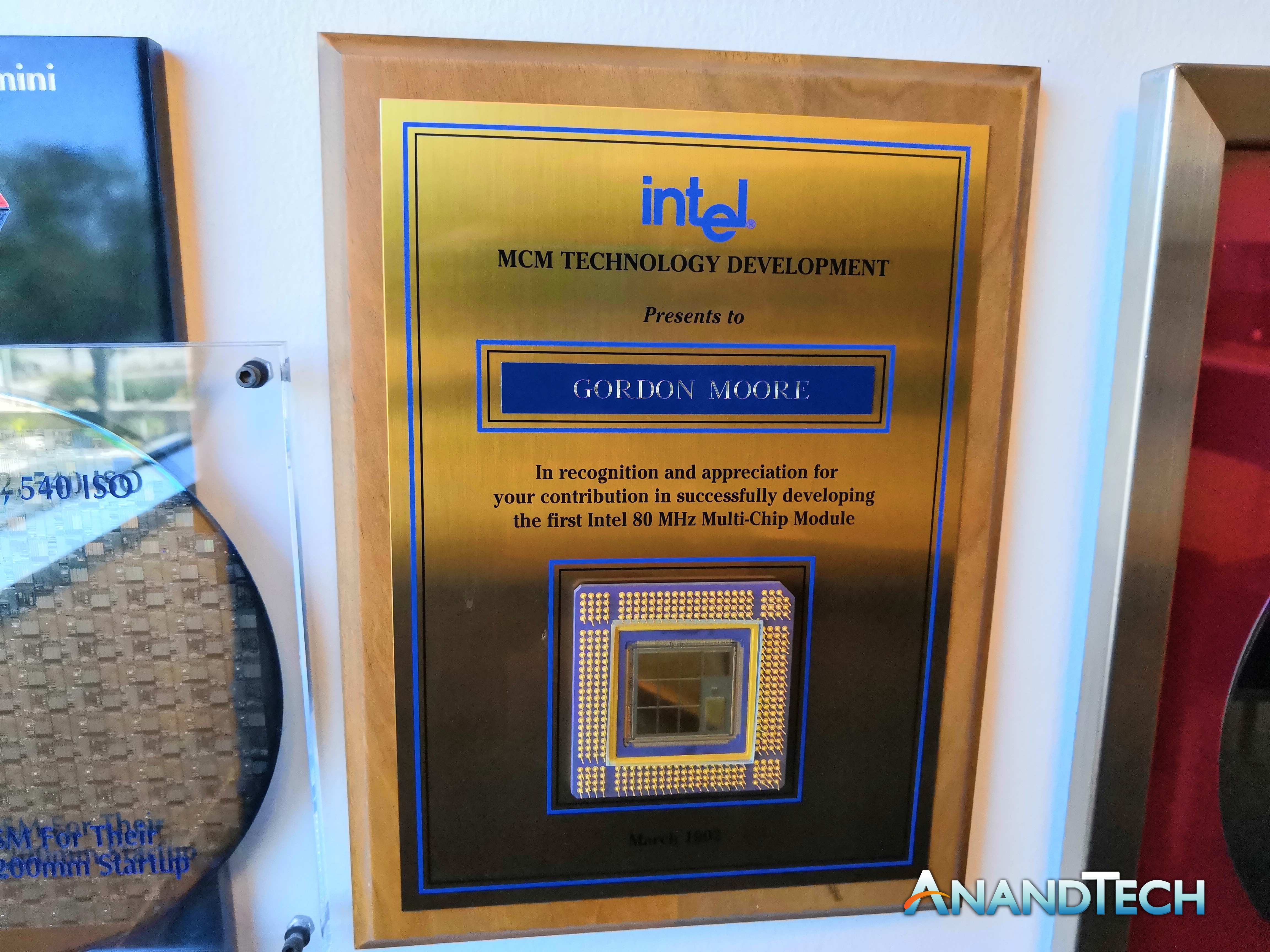
This next plaque, while not a wafer, will be interesting to users that have been following the recent Intel and AMD battle in the enterprise market. For all the talk of multi-chip modules, here is Intel’s first 80 MHz Multi-Chip Module from March 1992.
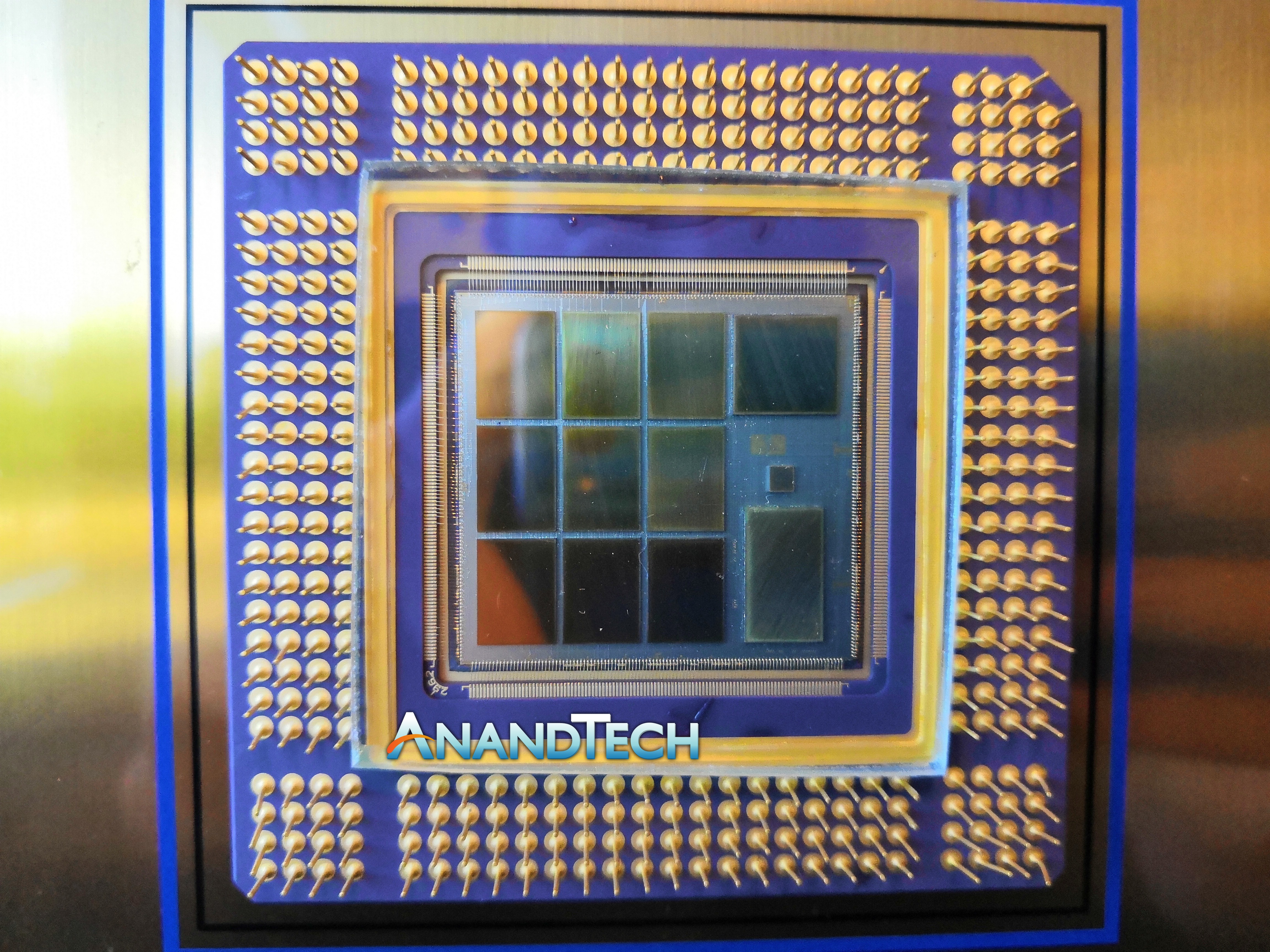
To get in really close, we see 12 or 13 separate chips all in the same package. Plenty of pins (in those days) to go with it of course.
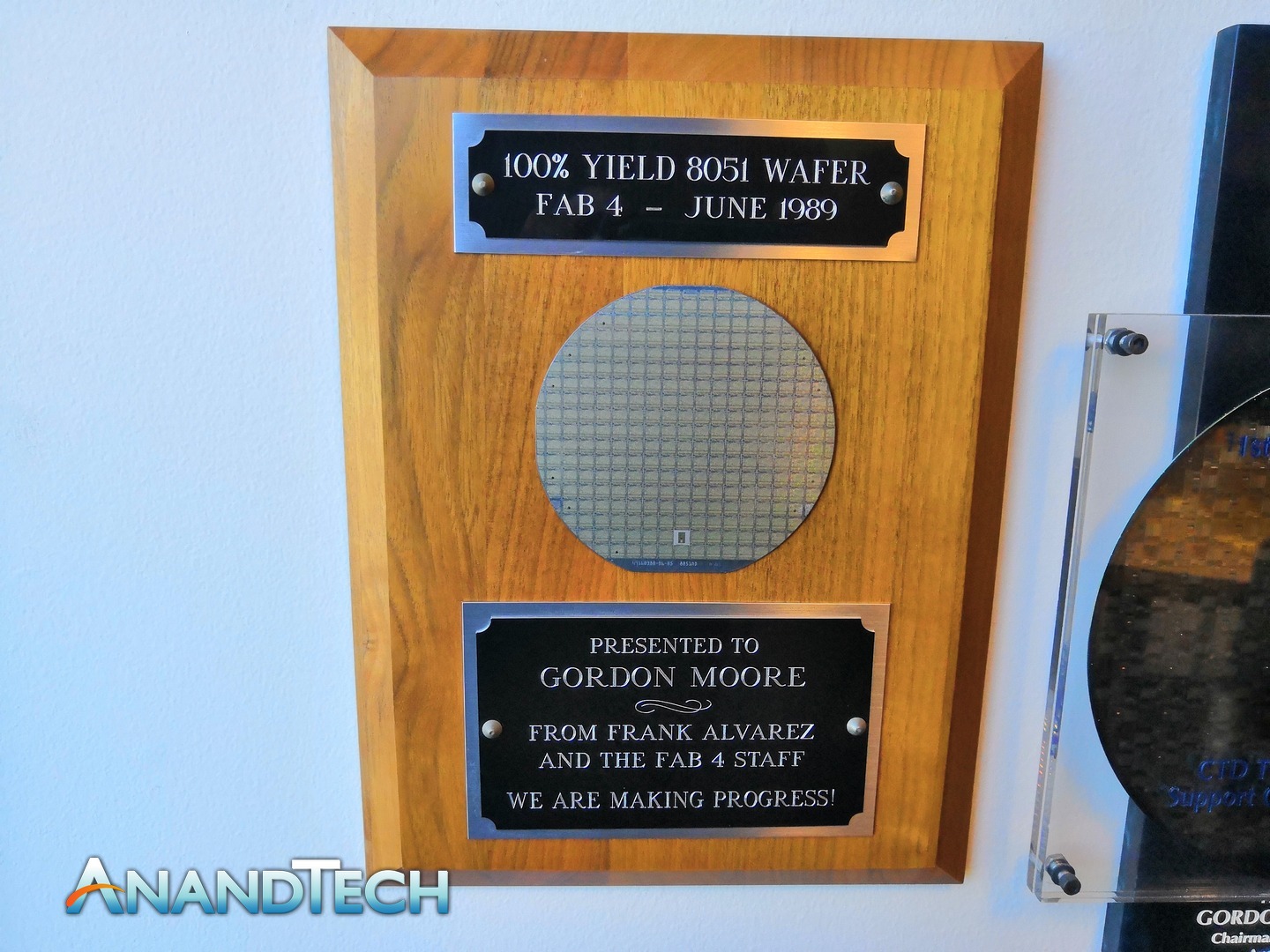
Because it represents the golden milestone in any manufacturing process, here is a plaque dedicated to Intel’s first 100% yielding wafer, from Fab 4 in June 1989. Fab 4 was in Aloha, Oregon, with this being the 8051. For any manufacturing process, making 100% yield is the result of hard work and chip design methodology, and I’m sure any major chip maker would love 100% on the latest processes in development today.
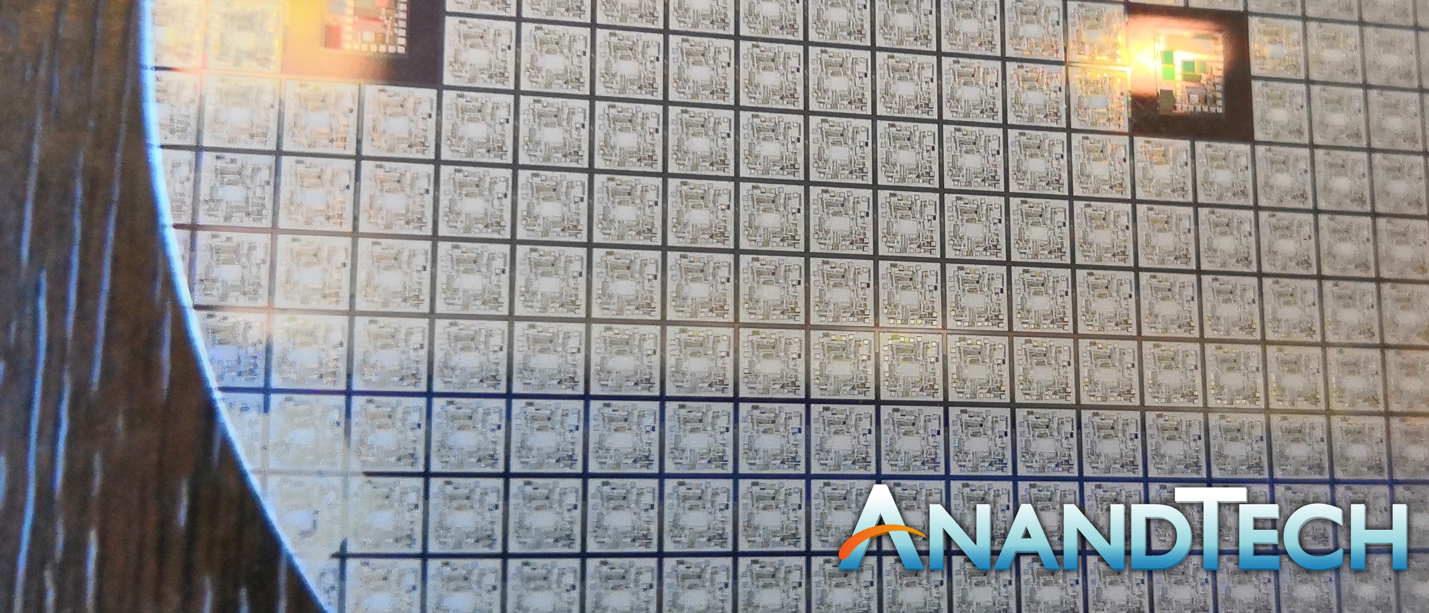
Here's a nice up close shot of one of Intel's Fab 2 three-inch wafers from 1985.
Aside from Moore's Wall of Wafers, here is Intel's Wall of More Moore. If that wasn't enough, there is always the gift shop.


37 Comments
View All Comments
ianmills - Thursday, May 31, 2018 - link
Good idea Mr.Stalin let's put all those scientists in jail who disobeyed the law!Bulat Ziganshin - Wednesday, May 30, 2018 - link
> the first processor capable of a single teraflop: Intel’s Pentium ProIan!!! Of course, it was first 1 TFLOP ***supercomputer*** and you can find on the photo that each processor was only 300 MFLOPS. The first Teraflop processor I know was Radeon 4870 from 2008
mode_13h - Friday, June 1, 2018 - link
What about this, from 2007 (and Intel, no less):https://en.wikipedia.org/wiki/Teraflops_Research_C...
ozzuneoj86 - Thursday, May 31, 2018 - link
A 720P 4:3 ratio LCD huh?guidryp - Thursday, May 31, 2018 - link
Looks similar to a 5:4(1280x1024) LCD I had back then.ozzuneoj86 - Thursday, May 31, 2018 - link
At first glance it looked more like a 4:3 to me. I have a 5:4 1280x1024 19" Dell on my workbench and its more square. The more I look at it, the more I think you're right that its 5:4. Still, its obviously not 16:9. Not a big deal, but... its hard to not notice this when a joke about screen resolution is made on a tech site.Why am I wasting my time writing about this? LOL
stadisticado - Friday, June 1, 2018 - link
He's been retired for a long time and likely hasn't had cause to sit at that desk for ~10 years for any reason. I'd expect outdated equipment.Jon Tseng - Thursday, May 31, 2018 - link
Huh cool. Presumably this is in the RNB right? What floor was it maybe I'll ask to see next time I'm there!Ian Cutress - Thursday, May 31, 2018 - link
It is - second floor.wrkingclass_hero - Thursday, May 31, 2018 - link
It's like he died 10 years ago