A Thought on Silicon Design: Intel’s LCC on HEDT Should Be Dead
by Ian Cutress on June 1, 2018 9:00 AM EST
In the past couple of weeks, we have been re-testing and re-analysing our second generation Ryzen 2000-series review. The extra time and writing, looking at the results and the state of the market, led me down some interesting thoughts, ideas, and concepts, about how the competitive landscape is set to look over the next 12-18 months.
Based on our Ryzen 2000-series review, it was clear that Intel’s 8-core Skylake-X product is not up to task. The Core i7-7820X wins in memory bandwidth limited tests because of the fact that it is quad channel over the dual channel competition, but it falls behind in almost every other test and it costs almost double compared to the other chips in benchmarks where the results are equal. It also only has 28 PCIe lanes, rather than the 40 that this chip used to have two generations ago, or 60 that AMD puts on its HEDT Threadripper processors.
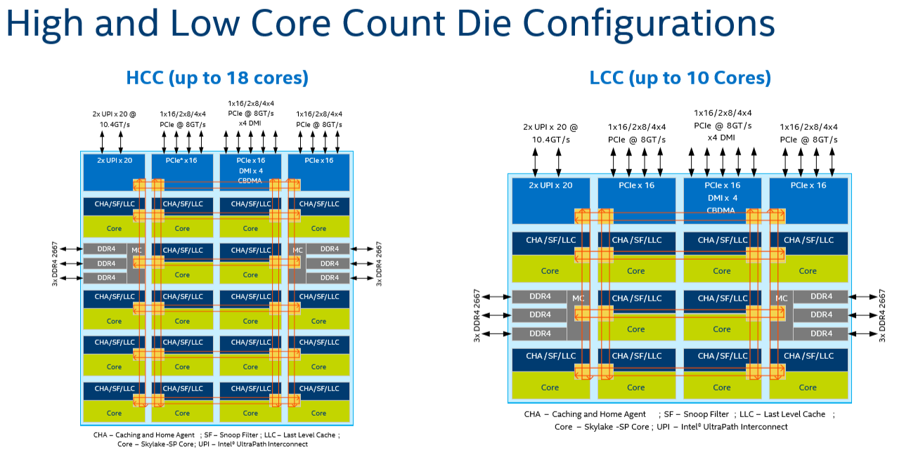
Intel uses its monolithic low-core-count (LCC) Xeon design for the 6-8-10 Skylake-X processors, as it has 10 cores in the silicon floor plan. AMD is currently highly competitive at 8 cores, with a much lower price point in the consumer space, making it hard for Intel to justify its 8-core Skylake-X design. Intel is also set to launch 8-core mainstream processors later this year, and is expected to extend its consumer ring-bus design from six-cores to eight-cores to do so, rather than transpose the 8-core LCC design using the latest Coffee Lake microarchitecture updates.
Because of all this, I am starting to be of the opinion that we will not see Intel release another LCC Xeon in the high-end desktop space in the future. AMD’s Threadripper HEDT processors run mainly at 12 and 16 cores, and we saw Intel ‘had to’* release its mid-range core count (called high core count, HCC) silicon design to compete.
*Officially Intel doesn’t consider its launch of 12-18 core Core i7/Core i9 processors a ‘response’ to AMD launching 16-core Threadripper processors. Many in the industry, due to the way the information came to light in spots and without a unified message, disagree.
In this high-end desktop space, looking to the future, AMD is only ever going to push higher and harder, and AMD has room to grow. The Infinity Fabric, between different dies on the same package, is now a tried and tested technology, allowing AMD to scale out its designs in future products. The next product on the block is Threadripper 2, a minor update over Threadripper but based on 12nm and presumably with higher frequencies and better latencies as well. We expect to see similar 3-10% uplift over the last generation, and it is likely to be up to 16 cores in a single package coming out later this year.

A der8auer delid photo
With AMD turning the screw, especially with rumors of more high performance cores in the future, several things are going to have to happen from Intel to compete:
- We will only see HCC processors for HEDT to begin
- The base LCC design is relegated to low-end Xeons, and
- Intel will design its next big microarchitecture update with EMIB* in mind
- To compete, Intel will have to put at least two dies on a single package.
*EMIB: Embedded Multi-Die Interconnect Bridge, basically an intra-package interposer to connect two chips at high bidirectional speed without a bulky interposer by inserting a micro-interposer in the package PCB/substrate. We currently see this technology on Intel’s Core with Radeon RX Vega (‘Kaby Lake-G’) processors in the latest Intel NUC.
For the next generation of server-class Xeon processors, called Cascade Lake-SP and which are expected to be coming either this year or early next (Intel hasn’t stated), we believe it to be a minor update over the current Skylake-SP. Thus for CL-SP, option (1)+(2) could happen then. If Intel wants to make the mainstream platform on Coffee Lake go up to 8 cores, the high-end desktop is likely to only see 10 cores and up. The simple way to do this is to put the HCC core design (could be up to 18 cores) and cut it as necessary for each processor. Unless Intel are updating the LCC design to 12 cores (not really feasible given the way the new inter-core mesh interconnect works, image below), Intel should leave the LCC for the low count Xeons and only put the HCC chips in the high-end desktop space.
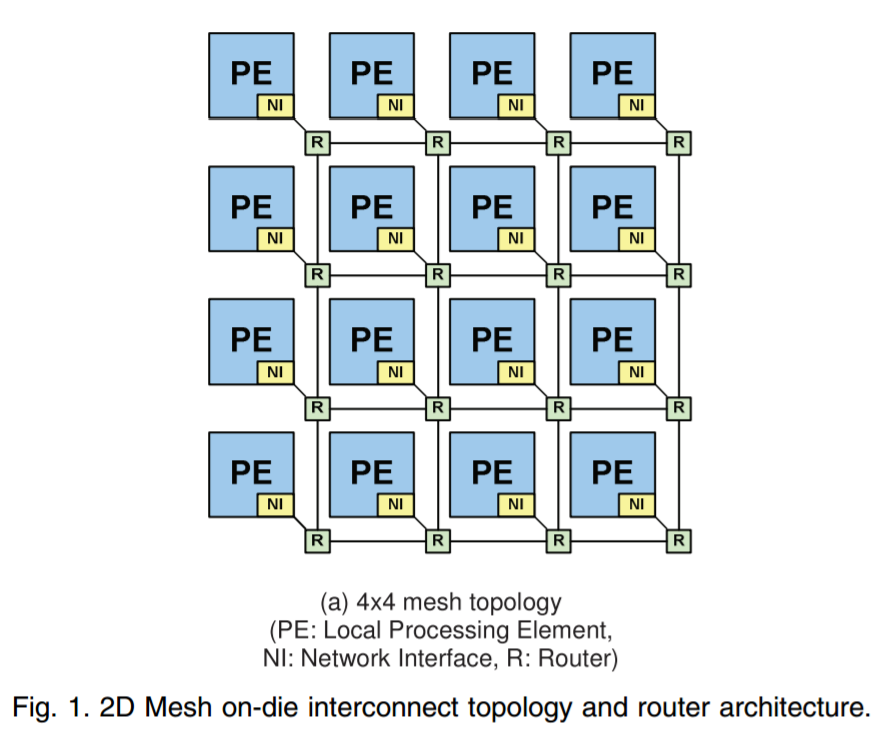
Representation of Intel's Mesh topology for its SP-class processors
Beyond CL-SP, for future generations, options (3)+(4) are the smarter paths to take. EMIB adds additional expense for packaging, but using two smaller dies should have a knock-on effect with better yields and a more cost effective implementation. Intel could also leave out EMIB and do an intra-package connection like AMD.
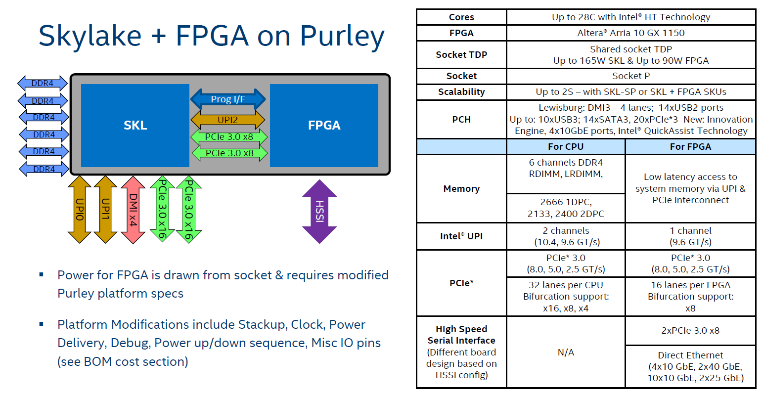
But one question is if Intel’s current library of interconnects, i.e. the ones that are competitors or analogues to AMD’s Infinity Fabric, are up to the task. Intel currently uses its UPI technology to connect between 2 socket, 4 socket and 8 socket platforms. Intel also uses it in the upcoming Xeon+FPGA products to combine two chips in a single package using an intra-package connection, but it comes at the expense of limiting those Xeon Gold processors down to two sockets rather than four (this is more a design thing of how the Xeon Gold has only 3 UPI connectors). But we will have to see if Intel can appropriately migrate UPI (or other technologies) across EMIB and over multiple dies in the same package. With the side of Intel, those dies might not need to be identical, like AMD, but as mentioned, AMD already has its Infinity Fabric in the market and selling today.
The question will be if Intel has had this in mind. We have seen ‘leaks’ in the past of Intel combining two reasonably high-core count chips into a single package, however we have never seen products like it in the market. If these designs are flying around Intel, which I’m sure they are, are they only for 10nm? Based on delays of 10nm, are Intel still waiting it out, or will they back-port the design as 14nm delays grow?
Intel’s Dr. Murthy Renduchintala, in a recent JP Morgan investment call, was clear that 10nm high volume manufacturing is set for 2019 (didn’t say when), but Intel is learning how to get more design wins within a node rather than waiting for new ones. I would not be surprised if this is one project that gets brought into 14nm in order to be competitive.
If Intel hasn’t done it by the time AMD launch Zen 2 on 7nm, the 10-15 year one-sided seesaw will tip the other way in the HEDT market.
Based on previous discussions from one member of the industry, I do not doubt that Intel might still win in the absolute raw money-is-no-object performance with its best high-end $10k+ parts. They are very good at that, and they have the money and expertise for these super halo, super high-bin monolithic parts. But if AMD makes the jump to Zen 2 and 7 nm before Intel comes to market with a post-Cascade Lake product on 10nm, then AMD is likely have the better, more aggressive, and more investment friendly product portfolio.
Competition is good.


30 Comments
View All Comments
MrSpadge - Friday, June 1, 2018 - link
To me this read like "they are trying to hide behind such BS, better judge them by what they actually do (and don't do)". I don't think it has to be more obvious than this.bortiz - Friday, June 1, 2018 - link
You mentioned the issue and skipped right over it. Traditionally Intel has had higher yields on large die than AMD (lower defect rate). This is not a design flaw on anyone's side, but prioritization. Intel sacrifices performance to get better yields (lower cost). So the cost savings AMD gets with smaller dies is more than Intel would get on comparable process technology (say 14 nm node).The big advantage for Intel is not in single socket systems, but multi-socket systems (high end). AMD has already used up it's socket count by connecting all the chips on a single substrate while Intel can still give you higher multiple socket count. With this Intel can scale to build larger systems.
Either way, this is good competition - which is great for everyone!!!
FreckledTrout - Friday, June 1, 2018 - link
Boritz, that post is confusing. What the heck does AMD has already used up it's socket count" mean? The Intel and AMD server chips you speak of all take up one socket. AMD connected a few chips together it's still a single socket, you can plug in multiple EPYC cpus into multi socket motherboards just like you can with Intel. Sure I can see intels large monolithic CPU's out performing AMD's approach on the high end but for none of the reasons you stated.MrSpadge - Friday, June 1, 2018 - link
More reasons to drop the LLC die or at least increase it's core count significantly:- at 6 - 10 cores the ring bus is obviously doing well, whereas Skylake-X is loosing performance and power efficiency. The mesh probably only starts to shine at over 20 cores or so. Otherwise they would have introduced it sooner.
- the HCC die at moderate core counts features a lower power density, so it can be cooled easier and hence be driven harder for workstation use.
zodiacfml - Friday, June 1, 2018 - link
Competition is not good. I still remember the days of AMD putting out good CPU designs but always come short due to Intel's superior node where AMD is behind by two generations. Lately, Intel is stubbornly waiting it out for 10nm, to save pennies, which makes it appear AMD is competing nicely. No wonder AMD or its CEO has been reserved with their comments for Ryzen, only positive statements that Ryzen will keep improving.jjj - Saturday, June 2, 2018 - link
Lisa Su said recently that Zen 2 is first in server and unless she misspoke, that means Zen 2 desktop won't be same die as server anymore.serendip - Sunday, June 3, 2018 - link
I'm curious as to the use cases for 16 cores on HEDT. If you're doing stuff like video encoding, wouldn't that be better served by GPUs? What desktop tasks are suitable for such high core counts?Vatharian - Sunday, June 3, 2018 - link
I strongly disagree on Intel's need to switch to mesh AMD-like topology. What's more important, they NOW would probably do anything to avoid such a step. They do have access to something much more aggressive: Intel has invested billions in joint-venture with Micron, and they do have access to highly efficient stacking technology. Dropping massive, like 2-4-8k wide ring bus under whole chip would allow Intel to basically rescale current designs, without regards to surface area taken by it. Literally no one else is capable of this approach.Also top tier for XCC Xeons can be further boosted by sticking few gigabytes of HBM beside it, as LLC.
I highly doubt that FPGA Xeons will hit mass market (or any market, even), first their TDP is obnoxiously high, like 270W+ per socket, and second, there is very high intro cost for usage - experience, tools, etc., so they will probably end up in direct customers' systems only. I guess FPGAs will instead trickle down to other products, like network infrastructure, specialized accelerators, and to some small degree, ML systems.
zepi - Monday, June 4, 2018 - link
I think there are some very lucrative FPGA markets available for example in financial industry. Investment banks have the money and willingness to pay for both HW and programming talent if they smell money.This kind of chips would most likely give super fat margins for Intel and I'm 110% sure that they will want to get them out sooner rather than later.
Kevin G - Tuesday, June 5, 2018 - link
Intel will continue to offer LCC dies as not every server application scales well with additional core count. In particular, these are also being sold to the markets where higher clock speeds for lower latency transactions are more important than raw throughput per socket (think high frequency trading).If Intel so desired, they could do a 5x4 mess arrangement to get a 14 core die: simply take the current 10 core schema and put an additional column of cores in the middle. (See the second picture in this article.) The MCC can take over the current XCC chip arrangement (5x6) in the future with the new XCC growing larger (7x6?).
There is another axis in which Intel can distinguish itself is by altering the amount of L3 cache between LCC, HCC and XCC. More cache means larger dies so this path would mean that the larger cache LCC chip would be similiar in size to the HCC chip if Intel were to really focus on this aspect. Say by putting 4 MB of L3 per tile vs the current 1.375 MB. Intel also has the option of introducing a medium core count chip (MCC?) into the mix if it makes sense.
I would also doubt that Intel is going to restrict the FPGA parts to two sockets due to the FPGA wanting a QPI/UPI link. One of the lesser known things is that these Xeon chips actually have controllers for 64 PCIe lanes on-die but the socket itself is only spec'd for 48 lanes externally. The spare 16 lanes go toward the on package Omnipath fabric of some models. If I were a betting man, I'd wager that Intel already has a spare QPI/UPI link on-die that isn't being used. These combo CPU+FPGA parts are something Intel hinted at before they purchased Altera so it has been in the works for sometime. Similarly, Intel at some point in the future is going to offer Nervana IP in the same package just like FPGA options.
Cascade Lake appears to be Sky Lake-SP with some errata fixed for Optane DIMM support. A move from 14+ nm to 14++ nm would also permit a slight clock speed boost but nothing earth shattering. This is what would be considered a new stepping back in the day.
Ice Lake is the design to look forward too. Intel at some point will start to leverage EMIB in the server space to expand their mesh topology. The difference in LCC, HCC and XCC products with EMIB would simply be the number of dies in the package dedicated just to CPU cores. This also permits Intel to expand their on-package options (Omnipath, FPGA, Nervana etc.) to flex EMIB packaging and use the same on-die mesh topology for cache coherency if it makes sense for a product. Lots of potential here but also several years away.