Intel Shows Xeon Scalable Gold 6138P with Integrated FPGA, Shipping to Vendors
by Ian Cutress on May 17, 2018 7:20 AM EST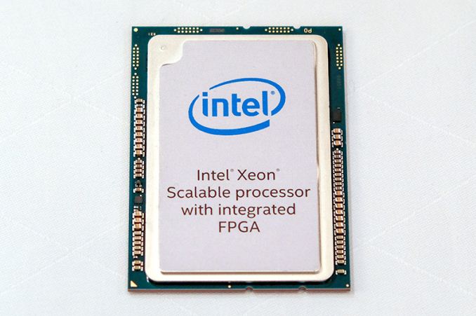
Part of the story behind the Xeon Scalable platform, built upon server-level Skylake processing cores with AVX-512 and a new mesh topology, was that the CPU was designed to be partnered with additional silicon in the same package. Out of the gate immediately were versions bundled with Intel’s OmniPath controller, allowing for networking fabric connections. There has always been expectation that Intel will launch a Xeon Scalable processor with an integrated Intel Altera FPGA on the same package, and now that expectation has become reality. Intel is now shipping its Xeon Gold 6138P processor with a built-in Altera Arria 10 GX 1150 FPGA.
Back at Supercomputing 2016, Intel demonstrated what supposed to be a Broadwell-based Xeon system with a built in FPGA into the same package, however no real details were given and the chip itself was not on display. This year, at Mobile World Congress (of all places), Intel had a demonstration system showing a Xeon Scalable processor with a built in FPGA into the same package, but again the chip was not on display, only a processor that supposedly had the chip in. I was not allowed to use my screwdriver to open the system up. The Intel attendant next to the system was discussing that the platform would help accelerate Edge Computing for data used by 5G networks, although discussions about the finer details of how many SKUs, the size of the FPGA, and other elements were met with a refusal to answer. As a result, I didn’t post anything at MWC; I could not confirm anything that was being said and Intel was not prepared to say any more.
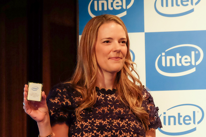
Lisa Spellman showing Intel Xeon + FPGA during Intel's Presentation at the Fujitsu Forum, Tokyo
Source: PC-Watch
Fast forward a couple of months, and over at PC-Watch are reporting that Intel has announced via its itpeernetwork hub (rather than its traditional PR outreach) the mass production of the Xeon Gold 6138P with an integrated Arria 10 GX 1150 FPGA, with some select customers already being sampled. The announcement states that Fujitsu is one of the Intel partners planning a system around this processor.
| Intel Xeon Gold: Adding an FPGA | ||
| AnandTech | Xeon Gold 6138 | Xeon Gold 6138P with Arria 10 FPGA |
| Socket | Socket P LGA 3647 |
Socket P LGA 3647 |
| Cores / Threads | 20 / 40 | 20 / 40 ? |
| Base Frequency | 2000 MHz | 2000 MHz ? |
| Turbo Frequency | 3700 MHz | 3700 MHz ? |
| PCIe Lanes | 48 | 32 |
| DRAM | Six Channels DDR4-2666 |
Six Channels DDR4-2666 |
| On-Package FPGA | - | Arria 10 GX 1150 |
| Logic Elements | - | 1150K (1.15m) |
| Embedded Memory | - | 53 Mb |
| UPI Links | Three | Two |
| TDP | 125 W | 125 W CPU 60 - 70 W FPGA 195 W Total ? |
| Price | $2612 | Arm, Leg |
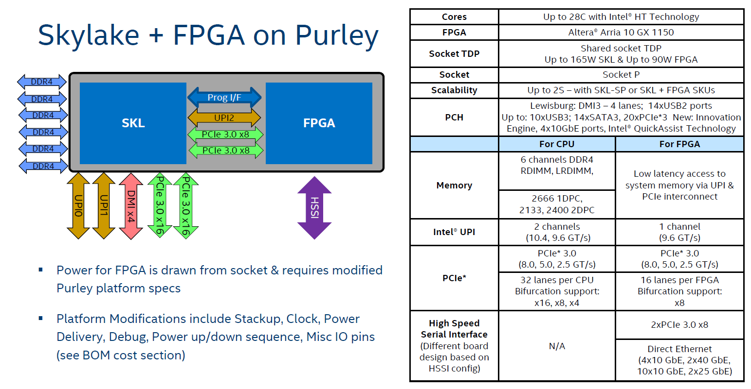
Intel is connecting the Xeon processor to the FPGA with 160 Gbps of bandwidth per socket (doesn’t state if this is bi-directional) using a cache coherent interconnect. From the way that we know that the Intel OmniPath Fabric connects in package to an Xeon, this connection likely implements a different protocol over the PCIe x16 interface reserved for in-package components, but also takes advantage of Intel’s Ultra-Path Interconnect (UPI) for cache coherency and access to data across the platform. This may mean that this reduces Xeon+FPGA setups to dual socket at best, if one UPI link from the processor is in use for the FPGA, however Intel did not provide briefings on the new parts to confirm this. We can confirm from an old Intel slide that the platform should be using a High Speed Serial Interface (HSSI) for connectivity; this slide also states that the new processors have different power specifications to standard Skylake-SP sockets, and as such the Xeon Gold 6138P is probably unlikely to be a drop in processor to current systems.
For this launch, Intel has built a virtual switching reference design, which uses the FPGA for infrastructure dataplane switching with virtual machines on the CPU implementing direct compute on the dataplane. Intel states that their reference design offers 3.2x better throughput and half the latency compared to a CPU-only solution when running the Open Virtual Switch framework. This test was measured through its DPDK forwarding performance. It was stated that at the Fujitsu Forum in Tokyo this week an OVS system with additional performance monitoring was on display.
The system under test was a 2P server using two of the new ‘Intel Xeon Gold 6138P with Integrated Arria 10 GX 1150 FPGA’ processors, 12x16 GB of DDR4-2666 (one DIMM per channel), and with an 100G Alaska network card from Marvell. Amusingly it says the system also had a PCIe 3.0 x10 slot, alongside a PCIe 3.0 x8 slot. 10 seems like a different number to normal.
Also in the announcement was a mention of Intel’s desire to offer a discrete FPGA solution with a faster high-bandwidth coherent connection, although details of this interconnect were not provided (it could be UPI through a physical discrete add-in card slot?). These discrete FPGA solutions will support code migration from code developed on the Xeon+FPGA system in this announcement as well as Altera’s Arria 10 GX acceleration cards.
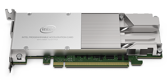
One of Intel's current Arria 10 GX 1150 Programmable Acceleration Cards
Wider availability of the Xeon Gold 6138P with Arria 10 is not yet known at this time. Interested parties are expected to get in contact with their Intel representative or OEM partner.
Source: Intel's ITPeerNetwork, PC-World (main image)


32 Comments
View All Comments
Arnulf - Friday, May 18, 2018 - link
"and in last year or so Intel purchase Altera."Meanwhile in this universe, Intel completed their acquisition of Altera in mid 2015.
UltraWide - Thursday, May 17, 2018 - link
LOLCajunArson - Thursday, May 17, 2018 - link
Get back to me when AMD finally implements a single piece of silicon that includes more than 8 cores. Since this mid-range chip has 20 cores just in the CPU, let's set the bar low for AMD and only require them to make a single 20 core product."Gluing" together two radically different chips with a high-speed interface in a single package is, yet again, years ahead of what AMD needs to do just to compete with a 2015 Broadwell part.
mga318 - Thursday, May 17, 2018 - link
I mean, yeah, it *is* "years ahead". Trouble is...the performance gap between even a 2013 Haswell and a Skylake chip isn't particularly huge when we consider how many years have gone by. "Years ahead" was a big deal when Moore's Law was still happening...but now? Meh.ZolaIII - Friday, May 18, 2018 - link
The hole idea about FPGA's is that they are scalable reprogrammable models of the hardware and how you don't need many general purpose CPU's paird with them (which is utterly stupid). FPGA's are good for both high parallel and moderate number of separate simultaneous tasks at the same time & both on separate & more optimal formed hardware blocks on programmable gate's so that they are the best fit for the task. So for instance if you want to accommodate more network IO requests sockets you either build an MIPS TSMP CPU or ASICS or a mix of them on the free gate mesh you don't build (nor use) huge X86 core's. Altera opted for instance for four A53 ARM core's for a reason as they needed general purpose core's only for basic tasks and autonomous operating.Santoval - Friday, May 18, 2018 - link
Zen 2 next year will probably have 6-core CCXs for 12-core dies, unless they abandon the CCX concept altogether. There's been talk about possible 64-core top server CPUs (4 x 16-core dies), but I don't think they could make 16-core dies with acceptable yields and reasonable sizes at 7nm, unless they develop them specifically for the server and datacenter market.AMD chose smaller dies with less cores because this is simply cheaper, with quite better yields. They have less money to burn than Intel and they outsource the manufacturing of CPUs and GPUs. The question is how much faster the link between the dies can become, while still being power efficient, since that is their multi-core performance bottleneck.
Ryzen 2000 series is faster than Broadwell in single thread performance btw, it is comparable to that of Skylake. Still behind Intel, but not so far behind.
ZolaIII - Friday, May 18, 2018 - link
It still is bad as it's not a complete SoC yet (lacks GPU, HMB) , their is still both IO and latency issue on glued garbage, besides bigger FPGA and less CPU cores are desired.patrickjp93 - Friday, May 18, 2018 - link
SOCs are not the answer for everything. Try harder.Santoval - Friday, May 18, 2018 - link
Intel does not use simple glue, they use *super* glue.igavus - Thursday, May 17, 2018 - link
Considering the price, does the five finger discount still apply?