Assessing Cavium's ThunderX2: The Arm Server Dream Realized At Last
by Johan De Gelas on May 23, 2018 9:00 AM EST- Posted in
- CPUs
- Arm
- Enterprise
- SoCs
- Enterprise CPUs
- ARMv8
- Cavium
- ThunderX
- ThunderX2
A little less than 2 years ago, we investigated the first Arm server SoC that had a chance to compete with midrange Xeon E5s: the Cavium ThunderX. The SoC showed promise, however the low single-threaded performance and some power management issues relegated the 48-core SoC to more niche markets such as CDN and Web caching. In the end, Cavium's first server SoC was not a real threat to Intel's Xeon.
But Cavium did not give up, and rightfully so: the server market is more attractive than ever. Intel's datacenter group is good for about 20 Billion USD (!) in revenue per year. And even better, profit margins are in 50% range. When you want to profits and cash flow, the server market far outpaces any other hardware market. So following the launch of the ThunderX, Cavium promised to bring out a second iteration: better power management, better single thread performance and even more cores (54).
The trick, of course, is actually getting to a point where you can take on the well-oiled machine that is Intel. Arm, Calxeda, Broadcom, AppliedMicro and many others have made many bold promises over the past 5 years that have never materialized, so there is a great deal of skepticism – and rightfully so – towards new Arm Server SoCs.
However, the new creation of underdog Cavium deserves the benefit of the doubt. Much has changed – much more than the name alone lets on – as Cavium has bought the "Vulcan" design from Avago. Vulcan is a rather ambitious CPU design which was originally designed by the Arm server SoC team of Broadcom, and as a result has a much different heritage than the original ThunderX. At the same time however, based on its experience from the ThunderX, Cavium was able to take what they've learned thus far and have introduced some microarchitectural improvements to the Vulcan design to improve its performance and power.
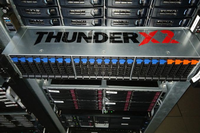
As a result, ThunderX2 is a much more "brainiac" core than the previous generation. While the ThunderX core had a very short pipeline and could hardly sustain 2 instructions per clock, the Vulcan core was designed to fetch 8 and execute up to 4 instructions per clock. It gets better: 4 simultaneous threads can be active (SMT4), ensuring that the wide back-end is busy most of the time. 32 of those cores at clockspeeds up to 2.5 GHz find a home in the new ThunderX2 SoC.
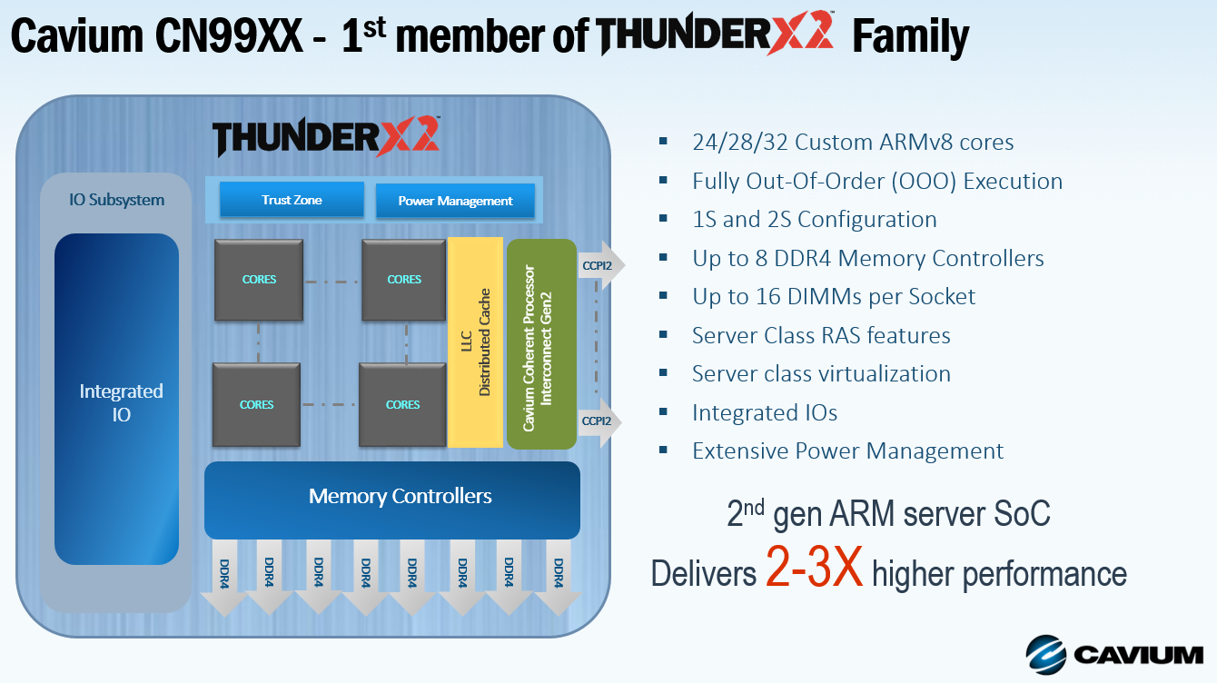
With up to 128 threads running and no less than eight DDR4 controllers, this CPU should be able to perform well in all server situations. In other words, while the ThunderX (1) was relegated to niche roles, the ThunderX2 is the first Arm server CPU that has a chance to break the server market open.


97 Comments
View All Comments
Wilco1 - Wednesday, May 23, 2018 - link
You might want to study RISC and CISC first before making any claims. RISC doesn't use more instructions than CISC. Vector instructions are actually quite similar on most ISAs. In fact I would say the Neon ones are more powerful and more general due to being well designed rather than added ad-hoc.HStewart - Wednesday, May 23, 2018 - link
The following site explain the difference using a simple multiply action, where a CISC architecture can do in single instruction, RISC would need to use multiple instructionshttp://www.firmcodes.com/difference-risc-sics-arch...
of course as time move on RISC chips added more complex operations and CISC also found ways to breaking more complex CISC instruction in smaller RISC like microcode increasing the chip ability to multitask the pipeline.
Wilco1 - Thursday, May 24, 2018 - link
The example was about load/store architecture, not multiply. In reality almost all instructions use registers (even on CISCs) since memory is too slow, so it's not a good example of what happens in actual code. The number of executed instructions on large applications is actually very close. The key reason is that compilers avoid all the complex instructions on x86 and mostly use register operations, not memory.Kevin G - Tuesday, May 29, 2018 - link
Raw instruction counts isn't a good metric to determine the difference between RISC and CISC, especially as both have evolved to include various SIMD and transactional extensions.The big thing for RISC is that it only supports a handful of instruction formats, generally all of the same length (traditionally 4 bytes)* and have alignment rules in place. x86 on the other hand leverages a series of prefixes to enhance instructions which permits length up to 15 bytes. On the flip side, there are also x86 instructions that consume a single byte. This also means x86 doesn't have the alignment rules that RISC chips generally adhere to.
*ARM does offer some compressed instruction formats in Thumb/Thumb2 but they those are also of a fixed length. 16 bit Thumb instructions are half size as 32 bit ARM instructions and have alignment rules as well.
Modern x86 is radically different internally than its philosophical lineage. x86 instructions are broken down into micro-ops which are RISC-like in nature. These decoded instructions are now being cached to bypass the complex and power hungry decode stages. Compare this to some ARM cores where some instructions do not have to be decoded. While having a simpler decode doesn't directly help with performance, it does impact power consumption.
However, I would differ and say that ARM's FPU and vector history has been rather troubled. Initially ARM didn't specify a FPU but rather a method to add coprocessors. This lead to 3rd parties producing ARM cores with incompatible FPUs. It wasn't until recently that ARM themselves put their foot down and mandated NEON as the one to rule them all, especially in 64 bit mode.
peevee - Wednesday, May 23, 2018 - link
The whole RISC vs CISC distinction is outdated for at least 20 years. Both now include a shi(p)load of instruction far outnumbering original CISC processors like 68000 and 8088 (from the epoch of the whole CISC vs RISC discussion), and both have a lot of architectural registers (which on speculative OoO CPUs are not even the same as real register files). ARMv8 for example includes NEON instructions, which is like... "AVX-128" (or SSE3 or smth).A lot of instructions means that both have to have huge decoders, which limits how small the CPU can be (because any reduction in other hardware which decrease performance faster than cost). For 64-bit ARMv8.2 it is very unlikely than an implementation can be made smaller than A55, and it is a huge core (in transistors) compared to even Pentium, let alone 8088.
HStewart - Wednesday, May 23, 2018 - link
I think the big difference between SIMD technologies - even though ARM has included they are not as wide as instructions as Intel or AMD. The following link appears to have a good comparison of chip SIMD comparison in size, To me in looks like AMD is on AVX level 8/16 instead of 16/32 in current chips while ARM including Neon is 4 Wide which is actually less than Core 2 SSE instructions from 10 years ago.https://stackoverflow.com/questions/15655835/flops...
It also interesting to note Ryzen stats - which I heard that AMD implement AVX 256 by combine two 128 together
One thing is that both Intel and AMD CPUs have grown a long ways since 20 years ago. In fact even todays Atom's can out rune most core-2 CPU's from 10 years - not my Xeon 5160 however.
ZolaIII - Thursday, May 24, 2018 - link
It's 2x128 NEON SIMD per ARM A75 core which goes into your smartphone.Even with smaller SIMD utilising TBL QC Centriq is able to beat up an Xerox Gold.
https://blog.cloudflare.com/neon-is-the-new-black/
Wilco1 - Thursday, May 24, 2018 - link
Modern Arm cores have 2-3 128-bit SIMD units, so 16-24 SP FLOPS/cycle. About half of Skylake theoretical flops, and yet they can match or beat Skylake on many HPC codes. Size is not everything...peevee - Thursday, May 24, 2018 - link
"ARM including Neon is 4 Wide which is actually less than Core 2 SSE instructions from 10 years ago"How is it less? It is the same 128 bits, 2x64 or 4x32 or 2x16...
And AMD combines 2 AVX-256 operations (not 2 128-bit SSEs) to get AVX-512.
patrickjp93 - Friday, May 25, 2018 - link
AMD does NOT have AVX-512. They combine 2 128s into a 256 on Ryzen, ThreadRipper, and Epyc.